

Why EUV Lithography is Critical for Future Semiconductor Devices
OCT 14, 20259 MIN READ
Generate Your Research Report Instantly with AI Agent
PatSnap Eureka helps you evaluate technical feasibility & market potential.
EUV Lithography Evolution and Objectives
Extreme Ultraviolet (EUV) lithography represents a revolutionary advancement in semiconductor manufacturing technology, emerging after decades of research and development efforts. The evolution of lithography technology has followed Moore's Law since the 1970s, progressing from mercury lamp-based systems through various generations of excimer laser technologies. Traditional deep ultraviolet (DUV) lithography, using 193nm wavelength light, reached its physical limits around 2010 despite multiple enhancement techniques such as immersion lithography and multi-patterning.
EUV lithography, operating at a dramatically shorter 13.5nm wavelength, emerged as the next critical evolutionary step to enable continued semiconductor scaling. This technology was first conceptualized in the 1980s, but required over three decades of intensive research to overcome fundamental physics and engineering challenges before becoming commercially viable. The primary objective of EUV lithography is to enable the continuation of Moore's Law by facilitating the production of increasingly smaller transistors and more densely packed integrated circuits.
The development timeline of EUV technology reveals persistent industry commitment despite numerous technical setbacks. Early EUV research programs began in the 1990s, with the first prototype tools appearing in the early 2000s. However, significant challenges in source power, mask technology, and photoresist performance delayed commercial implementation until 2019, when TSMC and Samsung began volume production of 7nm chips using EUV lithography.
A key objective of EUV lithography is process simplification. As traditional lithography reached its limits, manufacturers were forced to implement complex multi-patterning techniques that required numerous processing steps. EUV technology aims to reduce this complexity by enabling single-exposure patterning for critical layers, thereby improving yield and reducing manufacturing costs despite the higher initial investment in EUV equipment.
Beyond current applications, EUV lithography targets enabling future semiconductor nodes below 3nm, supporting the development of next-generation computing architectures. The technology roadmap includes high-NA (numerical aperture) EUV systems currently under development, which will further extend resolution capabilities to support semiconductor scaling into the 2030s.
The ultimate objective of EUV lithography extends beyond mere dimensional scaling. It aims to enable entirely new device architectures such as gate-all-around transistors, integrated photonics, and 3D stacking technologies that will form the foundation of future computing systems. These advanced devices are essential for meeting the exponentially growing computational demands of artificial intelligence, quantum computing, and other emerging technologies that will define the next era of semiconductor innovation.
Semiconductor Market Demands for Advanced Lithography
The semiconductor industry is experiencing unprecedented demand for advanced lithography solutions, driven by the relentless pursuit of Moore's Law and the continuous miniaturization of semiconductor devices. As transistor dimensions shrink below 10nm, traditional deep ultraviolet (DUV) lithography reaches its physical limitations, creating a critical market need for Extreme Ultraviolet (EUV) lithography technology.
Market analysis reveals that the global semiconductor industry, valued at approximately $556 billion in 2021, is projected to reach $1 trillion by 2030, with advanced nodes representing the highest growth segment. This expansion is fueled by explosive demand across multiple sectors including high-performance computing, artificial intelligence, autonomous vehicles, and 5G/6G telecommunications infrastructure.
Leading semiconductor manufacturers face increasing pressure to deliver chips with higher performance, lower power consumption, and greater functionality in smaller form factors. These market requirements directly translate to demand for lithography systems capable of producing ever-finer circuit patterns. Industry surveys indicate that 70% of semiconductor manufacturers consider advanced lithography capabilities essential for maintaining competitive advantage in premium market segments.
The economic implications of EUV adoption are substantial. While EUV systems represent significant capital investments (each system costs upwards of $150 million), the technology enables critical cost efficiencies through process simplification. Traditional multi-patterning approaches using DUV require 2-4 times more process steps than single-exposure EUV for equivalent feature sizes, resulting in higher manufacturing costs and lower yields at advanced nodes.
Consumer electronics markets particularly drive demand for advanced lithography, with smartphone processors, high-bandwidth memory, and advanced logic chips requiring 7nm processes and below. The data center segment similarly demands cutting-edge semiconductor technology to support exponential growth in cloud computing and AI workloads.
Geopolitical factors further intensify market demand for advanced lithography capabilities. Nations increasingly view semiconductor manufacturing self-sufficiency as a strategic imperative, spurring government investments exceeding $100 billion globally to establish domestic advanced chip production capabilities, all requiring EUV technology.
The transition to advanced packaging technologies like chiplets and 3D integration creates additional demand for high-precision lithography. These approaches require extremely accurate alignment and interconnection between multiple chips, necessitating the resolution capabilities that only EUV can provide.
Market forecasts indicate EUV lithography equipment sales will grow at a CAGR of 16% through 2026, reflecting the critical nature of this technology for future semiconductor manufacturing and the industry's commitment to continued miniaturization despite escalating technical challenges and costs.
EUV Technology Status and Implementation Barriers
Extreme Ultraviolet (EUV) lithography represents a significant technological breakthrough in semiconductor manufacturing, yet its global implementation faces substantial challenges. Currently, EUV technology has reached commercial viability with ASML's delivery of production-ready systems to leading semiconductor manufacturers including TSMC, Samsung, and Intel. These systems operate at a 13.5nm wavelength, enabling the production of chips at 7nm nodes and below.
Despite this progress, EUV technology confronts several critical barriers. The most significant challenge remains the power source efficiency. Current EUV light sources convert only about 5% of input energy into usable EUV radiation, resulting in substantial energy waste and thermal management issues. This inefficiency directly impacts throughput capabilities, with current systems processing approximately 125-140 wafers per hour—significantly lower than the 250+ wafers achieved with traditional immersion lithography.
Mask defectivity presents another major obstacle. EUV masks are fundamentally different from traditional optical masks, utilizing reflective rather than transmissive designs. The complexity of these masks makes them highly susceptible to defects during manufacturing and handling. Even microscopic particles or imperfections can cause critical pattern failures, and inspection technologies for these defects remain inadequate for high-volume manufacturing requirements.
The economics of EUV implementation create substantial barriers to widespread adoption. Each EUV lithography system costs approximately $150-200 million, with significant additional expenses for facility modifications, specialized infrastructure, and maintenance. This represents a capital investment 2-3 times higher than previous generation lithography tools, limiting adoption to only the most financially capable semiconductor manufacturers.
Technical infrastructure requirements further complicate implementation. EUV systems demand extraordinary environmental stability, including precise temperature control (±0.001°C), vibration isolation systems, and specialized vacuum environments. These requirements often necessitate purpose-built facilities, adding to the already substantial implementation costs.
Photoresist technology for EUV remains suboptimal, with current materials struggling to balance sensitivity, resolution, and line edge roughness. The limited photon count in EUV exposure creates fundamental physical challenges for resist chemistry that have not been fully resolved, impacting yield and performance consistency.
Geographically, EUV technology development and implementation remain concentrated in specific regions. The Netherlands (ASML), Japan (resist and mask technologies), and the United States (light source development) dominate the supply chain, while implementation is primarily occurring in Taiwan, South Korea, and the United States, creating potential geopolitical vulnerabilities in the global semiconductor ecosystem.
Current EUV Implementation Strategies and Solutions
01 EUV lithography system design and components
EUV lithography systems incorporate specialized components designed to work with extreme ultraviolet light. These systems include projection optics, illumination systems, and reflective masks that operate in vacuum environments. The design focuses on achieving high resolution patterning while managing thermal effects and maintaining precise alignment of optical elements for nanometer-scale semiconductor manufacturing.- EUV Lithography System Components: EUV lithography systems consist of specialized components designed to work with extreme ultraviolet light. These include EUV light sources, reflective optics (as opposed to refractive optics used in conventional lithography), specialized masks, and precise positioning systems. The systems must operate in vacuum conditions since EUV light is absorbed by air. Advanced control systems are required to maintain the precise alignment and stability needed for nanometer-scale feature production.
- EUV Light Source Technology: EUV lithography requires specialized light sources that can generate extreme ultraviolet radiation at a wavelength of approximately 13.5nm. These sources typically use laser-produced plasma or discharge-produced plasma technologies where high-energy lasers or electrical discharges strike targets (often tin droplets) to create EUV-emitting plasma. The light source systems include sophisticated debris mitigation, collection optics, and dose control mechanisms to deliver consistent illumination for the lithography process.
- EUV Mask Technology and Defect Management: EUV masks differ significantly from conventional photomasks, using reflective rather than transmissive designs with multiple layers of alternating materials to reflect EUV radiation. The masks require exceptional flatness and defect control at the nanometer scale. Advanced inspection and repair technologies are employed to identify and address defects that could impact pattern transfer. Pellicle technologies are being developed to protect EUV masks from contamination during use, though this presents unique challenges due to the EUV wavelength.
- EUV Resist and Process Development: Specialized photoresist materials are required for EUV lithography that can respond to the 13.5nm wavelength radiation while providing high resolution, sensitivity, and low line edge roughness. These resists often employ chemical amplification mechanisms and may include metal-containing compounds to enhance EUV absorption. The development process must account for secondary electron effects unique to EUV exposure. Post-exposure processing techniques are optimized to enhance pattern fidelity and reduce defects in the final structures.
- Computational and Control Systems for EUV Lithography: Advanced computational methods are essential for EUV lithography, including optical proximity correction, source mask optimization, and inverse lithography techniques tailored to EUV-specific challenges. Machine learning algorithms are increasingly employed to optimize process parameters and predict system behavior. Sophisticated control systems manage the complex interplay between subsystems, maintaining precise alignment, temperature stability, and timing synchronization required for successful EUV lithography. These systems must compensate for various physical effects specific to EUV wavelengths.
02 Contamination control and mitigation in EUV systems
Contamination control is critical in EUV lithography due to the sensitivity of optical components to molecular and particulate contamination. Various techniques are employed to prevent and mitigate contamination, including specialized cleaning methods, protective pellicles, gas purging systems, and contamination barriers. These approaches help maintain the reflectivity of mirrors and extend the lifetime of expensive EUV components.Expand Specific Solutions03 EUV source technology and power optimization
EUV light sources, typically based on laser-produced plasma or discharge-produced plasma, are essential components that determine system throughput. Innovations focus on increasing source power, stability, and conversion efficiency while reducing debris generation. Advanced collector designs and plasma confinement techniques help maximize the usable EUV radiation for high-volume manufacturing applications.Expand Specific Solutions04 Mask technology and defect inspection for EUV
EUV masks require specialized multilayer reflective coatings and precise patterning to achieve the desired imaging performance. Advanced inspection and repair technologies are developed to detect and address defects that could impact pattern transfer. Innovations include actinic inspection tools, phase defect management, and compensation techniques to ensure mask quality meets the stringent requirements of EUV lithography.Expand Specific Solutions05 Process control and overlay accuracy in EUV lithography
Achieving precise overlay and critical dimension control in EUV lithography requires sophisticated metrology and process control methods. Systems incorporate advanced alignment sensors, real-time feedback mechanisms, and computational models to compensate for process variations. Thermal management and mechanical stability solutions help maintain nanometer-level accuracy during exposure processes for complex semiconductor device manufacturing.Expand Specific Solutions
Leading EUV Equipment Manufacturers and Chip Producers
EUV lithography represents a critical inflection point in semiconductor manufacturing, with the market currently in a growth phase driven by increasing demand for advanced chips. The global EUV market is expanding rapidly, projected to reach significant scale as leading manufacturers transition to sub-7nm nodes. Technologically, industry leaders like TSMC, Samsung Electronics, and Intel are at the forefront of EUV adoption, while equipment suppliers ASML, Tokyo Electron, and Applied Materials control the ecosystem. Chinese players including SMIC face challenges accessing this technology due to export controls. Academic institutions like Tsinghua University and research organizations are actively developing alternative approaches, though commercial viability remains years away. EUV adoption represents both a technological breakthrough and strategic advantage in the global semiconductor competition.
Taiwan Semiconductor Manufacturing Co., Ltd.
Technical Solution: TSMC has pioneered EUV lithography implementation in high-volume manufacturing, beginning with their 7nm+ process and fully deploying it in their 5nm technology node. Their approach involves a comprehensive EUV infrastructure including specialized photoresist materials, mask technologies, and process optimization. TSMC utilizes ASML's NXE series EUV scanners, particularly the NXE:3400B and more advanced models, achieving resolution capabilities below 13nm. Their EUV implementation strategy includes multi-patterning techniques for critical layers, specialized pellicles for mask protection, and advanced computational lithography to enhance pattern fidelity. TSMC has reported significant benefits including a 20% reduction in mask layers compared to traditional multi-patterning approaches, resulting in simplified process flows and improved yields. Their EUV deployment has enabled transistor density improvements of approximately 1.8x when transitioning from 7nm to 5nm nodes, with plans to further enhance EUV utilization in their 3nm and 2nm technology roadmaps.
Strengths: Industry-leading implementation expertise with proven high-volume manufacturing capability; comprehensive infrastructure integration; demonstrated yield management. Weaknesses: High capital expenditure requirements (each EUV scanner costs >$150M); ongoing challenges with EUV power source stability and throughput optimization; dependency on limited equipment suppliers.
Tokyo Electron Ltd.
Technical Solution: Tokyo Electron (TEL) has developed specialized equipment and process solutions to support EUV lithography implementation in semiconductor manufacturing. Their approach focuses on the critical pre- and post-exposure processing steps that are essential for successful EUV lithography. TEL's CLEAN TRACK™ LITHIUS Pro™ Z coater/developer system has been specifically optimized for EUV processes, addressing the unique challenges of EUV photoresist handling, including thickness uniformity control within ±3Å across 300mm wafers. Their technology includes advanced thermal processing modules with precise temperature control (±0.3°C) critical for EUV resist performance optimization. TEL has also developed specialized etching solutions compatible with EUV patterning requirements, including their Tactras™ system which provides highly selective pattern transfer capabilities essential for EUV-defined features. Their process solutions incorporate advanced metrology and inspection integration to enable closed-loop control for EUV processes, helping manufacturers achieve the tight process windows required. TEL's equipment incorporates specialized contamination control technologies designed specifically for the unique particle and molecular contamination challenges associated with EUV processes.
Strengths: Comprehensive track and etch solutions specifically optimized for EUV processes; established relationships with major semiconductor manufacturers; complementary technology to ASML's exposure tools. Weaknesses: Not a direct provider of EUV exposure tools, limiting full process control; dependent on EUV adoption rates by manufacturers; faces competition from other track/process equipment providers.
Key EUV Patents and Technical Breakthroughs
Protection layer on low thermal expansion material (LTEM) substrate of extreme ultraviolet (EUV) mask
PatentActiveUS12001132B2
Innovation
- A protection layer is deposited on the LTEM substrate, functioning as an etch stop and reducing particle generation during EUV irradiation, while retaining some reflective multilayers to maintain high reflectivity and control critical dimension errors.
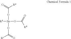
Semiconductor photoresist composition and method of forming patterns using the composition
PatentActiveUS12013635B2
Innovation
- A semiconductor photoresist composition is developed, comprising a condensed product from a condensation reaction between an organotin compound and organic acid compounds, which enhances sensitivity and storage stability, and includes a solvent and optional additives like surfactants and crosslinking agents, forming a pattern with improved aspect ratio and resistance to moisture.
Supply Chain Resilience for EUV Components
The supply chain for EUV lithography components represents one of the most complex and vulnerable aspects of advanced semiconductor manufacturing. The extreme precision required for EUV systems has created a highly specialized supply network with significant concentration risks. ASML, as the sole manufacturer of EUV lithography machines, depends on a network of over 5,000 suppliers across more than 60 countries, creating multiple potential points of failure.
Critical components such as the laser-produced plasma source, which generates EUV light by firing laser pulses at tin droplets, are manufactured by only a handful of specialized companies. Similarly, the ultra-precise mirrors coated with multilayer reflective materials come from a limited number of suppliers with the necessary expertise. This concentration creates inherent vulnerabilities in the supply chain.
Geopolitical tensions have further complicated EUV supply chain resilience. Export controls and technology restrictions between major semiconductor-producing nations have created uncertainty around the availability of critical components. The COVID-19 pandemic exposed additional weaknesses, as disruptions in global logistics and manufacturing capacity led to extended lead times for EUV systems, sometimes exceeding 18 months.
To address these vulnerabilities, leading semiconductor manufacturers have implemented several strategies. Vertical integration has become increasingly common, with companies like Intel and Samsung investing in their own component manufacturing capabilities. Strategic stockpiling of critical parts has also emerged as a risk mitigation approach, though this ties up significant capital and creates inventory management challenges.
Geographical diversification represents another key strategy, with companies establishing redundant supply sources across different regions. However, the specialized nature of EUV components limits the effectiveness of this approach, as few alternative suppliers possess the necessary technical capabilities.
Industry-government partnerships have also emerged as a critical element of supply chain resilience. Major semiconductor-producing nations have implemented policies to support domestic manufacturing capacity for critical EUV components through subsidies, tax incentives, and research funding. These initiatives aim to reduce dependency on single sources and create more robust supply networks.
Looking forward, the industry is exploring advanced manufacturing techniques like additive manufacturing for certain components, which could potentially enable more distributed production models. Additionally, design standardization efforts may help reduce customization requirements and improve interchangeability of parts across different EUV systems, further enhancing supply chain flexibility.
Environmental Impact of EUV Manufacturing Processes
The environmental impact of EUV lithography represents a significant consideration in semiconductor manufacturing. EUV systems consume substantial energy, with a single EUV lithography machine requiring approximately 1 megawatt of power during operation—equivalent to the electricity needs of about 800 households. This high energy demand stems primarily from the complex process of generating EUV light, where tin droplets are vaporized by high-powered CO2 lasers to create plasma that emits the required 13.5nm wavelength radiation.
Water usage presents another environmental challenge, as EUV systems require ultra-pure water for cooling and cleaning processes. A typical semiconductor fabrication facility utilizing EUV technology may consume millions of gallons of water daily, placing significant pressure on local water resources, particularly in water-stressed regions where many semiconductor manufacturing facilities are located.
The production of EUV equipment involves rare earth elements and specialized materials whose mining and processing carry substantial environmental footprints. Additionally, the gases used in EUV lithography processes include perfluorocarbons (PFCs) and sulfur hexafluoride (SF6), which have global warming potentials thousands of times greater than carbon dioxide when released into the atmosphere.
Waste management poses further challenges, as EUV processes generate various waste streams including used tin, contaminated water, and chemical byproducts that require specialized handling and disposal. The semiconductor industry has implemented advanced waste treatment systems, but the increasing complexity of EUV processes continues to present new waste management challenges.
Despite these environmental concerns, EUV lithography offers certain sustainability advantages compared to previous technologies. The improved precision reduces material waste through fewer manufacturing steps and rework requirements. Additionally, the higher transistor densities enabled by EUV technology result in more energy-efficient devices throughout their lifecycle, potentially offsetting some of the manufacturing impacts.
Leading semiconductor manufacturers have recognized these environmental challenges and are implementing mitigation strategies. These include investing in renewable energy sources to power EUV facilities, developing closed-loop water recycling systems, researching alternative process chemicals with lower environmental impacts, and designing more energy-efficient EUV systems. ASML, the primary manufacturer of EUV equipment, has committed to circular economy principles in their manufacturing processes and equipment design to minimize environmental footprint.
Unlock deeper insights with PatSnap Eureka Quick Research — get a full tech report to explore trends and direct your research. Try now!
Generate Your Research Report Instantly with AI Agent
Supercharge your innovation with PatSnap Eureka AI Agent Platform!