Why EUV Lithography Is Key to Breakthroughs in Miniaturization
OCT 14, 20259 MIN READ
Generate Your Research Report Instantly with AI Agent
Patsnap Eureka helps you evaluate technical feasibility & market potential.
EUV Lithography Evolution and Miniaturization Goals
Extreme Ultraviolet (EUV) lithography represents a revolutionary advancement in semiconductor manufacturing technology, marking a significant milestone in the ongoing quest for miniaturization. The evolution of lithography technology has been driven by Moore's Law, which predicted the doubling of transistor density approximately every two years. Traditional deep ultraviolet (DUV) lithography, using 193nm wavelength light, reached its physical limits around the 7nm node, necessitating the development of EUV technology with its much shorter 13.5nm wavelength.
The journey toward EUV lithography began in the late 1990s when semiconductor industry leaders recognized the impending limitations of DUV technology. Early research focused on overcoming fundamental challenges, including the development of suitable light sources, mirrors, and photoresist materials capable of working with such short wavelengths. The technology underwent extensive development phases, with significant breakthroughs occurring in the 2010s that finally made commercial implementation viable.
EUV lithography aims to enable the continuation of Moore's Law by facilitating the production of increasingly smaller transistors and circuit elements. The primary goal is to achieve feature sizes below 7nm while maintaining manufacturing efficiency and economic viability. This technology targets a resolution capability of approximately 13nm, representing a substantial improvement over previous lithography methods and opening pathways to 5nm, 3nm, and potentially even smaller process nodes.
Beyond mere size reduction, EUV lithography addresses several critical objectives in semiconductor manufacturing. It aims to reduce multi-patterning steps required in DUV lithography, thereby simplifying the manufacturing process and potentially reducing costs despite the higher initial investment in EUV equipment. The technology also seeks to improve yield rates and reduce defect densities at advanced nodes, which becomes increasingly challenging as feature sizes shrink.
The miniaturization enabled by EUV lithography serves broader technological goals across multiple industries. In computing, it facilitates higher performance, greater energy efficiency, and increased functionality in the same or smaller form factors. For mobile devices, it enables more powerful processors with lower power consumption. In data centers, it allows for higher density computing resources to support growing AI and cloud computing demands.
Looking forward, the EUV roadmap includes further wavelength reduction (High-NA EUV), improved photoresist sensitivity, and enhanced manufacturing techniques. These advancements aim to extend semiconductor scaling beyond current projections, potentially enabling process nodes as small as 1nm in the coming decade and supporting the next generation of computing paradigms including quantum computing interfaces, neuromorphic computing, and advanced AI accelerators.
Market Demand for Advanced Semiconductor Nodes
The semiconductor industry's demand for advanced nodes has been experiencing exponential growth, driven primarily by the increasing computational requirements of artificial intelligence, high-performance computing, and data centers. Market research indicates that the global semiconductor industry reached approximately $600 billion in 2023, with advanced nodes (7nm and below) representing the fastest-growing segment at over 20% annual growth rate.
This surge in demand stems from several interconnected market forces. First, the proliferation of AI applications has created unprecedented requirements for processing power. Training large language models and neural networks demands chips with billions of transistors operating at maximum efficiency, which only advanced nodes can deliver. Companies like NVIDIA, AMD, and Intel are competing intensely to capture this high-margin market segment.
Mobile computing represents another significant driver for advanced nodes. As smartphones and tablets continue to incorporate more sophisticated features such as on-device AI processing, augmented reality, and high-resolution displays, the need for more powerful yet energy-efficient processors has become paramount. Apple's move to design its own silicon using TSMC's advanced nodes exemplifies this trend.
The automotive sector has emerged as a surprising growth area for advanced semiconductor nodes. Modern vehicles incorporate dozens of electronic control units, with autonomous driving features requiring specialized AI processors manufactured on advanced nodes. Industry projections suggest that semiconductor content in premium vehicles could exceed $1,000 per vehicle by 2025, with a significant portion allocated to advanced node processors.
Cloud infrastructure providers represent another major demand source. As businesses migrate to cloud-based solutions, hyperscalers like Amazon Web Services, Microsoft Azure, and Google Cloud are investing heavily in data centers equipped with cutting-edge processors. These companies are increasingly designing custom silicon tailored to their specific workloads, all requiring the most advanced manufacturing processes available.
The Internet of Things (IoT) ecosystem, while often associated with simpler chips, is creating demand for edge computing devices that require advanced node processors to handle complex processing tasks locally rather than in the cloud. This trend is particularly evident in industrial IoT applications where real-time processing is critical.
Geopolitical factors have further complicated the market landscape. The strategic importance of semiconductor technology has prompted governments worldwide to invest in domestic chip manufacturing capabilities, with particular emphasis on advanced nodes. The CHIPS Act in the United States and similar initiatives in Europe and Asia represent multi-billion dollar commitments to securing advanced semiconductor manufacturing capacity.
EUV Technology Status and Implementation Challenges
Extreme Ultraviolet (EUV) lithography represents a revolutionary advancement in semiconductor manufacturing technology, currently deployed in leading-edge production nodes at 7nm and below. The global implementation of EUV technology remains limited to a select few semiconductor manufacturers including TSMC, Samsung, and Intel, with ASML maintaining a monopoly as the sole supplier of EUV lithography equipment.
Despite its transformative potential, EUV technology faces significant implementation challenges. The primary obstacle remains the power source - generating sufficient EUV light intensity requires complex laser-produced plasma systems that convert tin droplets into EUV radiation at 13.5nm wavelength. Current power sources struggle to achieve the ideal 250W output required for optimal production throughput, with most systems operating between 170-200W, creating a persistent bottleneck in manufacturing efficiency.
Mask infrastructure presents another critical challenge. EUV masks require fundamentally different manufacturing processes compared to traditional optical lithography masks. The absence of pellicles (protective covers) that can withstand EUV's intense energy creates defect risks, while mask inspection and repair technologies remain less mature than their optical counterparts. These factors contribute to higher defect rates and yield challenges in early implementation phases.
The economics of EUV implementation cannot be overlooked. Each EUV lithography machine costs approximately $150-200 million, representing an extraordinary capital investment. Additionally, the operational costs including maintenance, specialized facilities, and highly trained personnel further increase the total cost of ownership. This economic barrier restricts EUV adoption to only the largest semiconductor manufacturers with sufficient capital resources.
Technical integration challenges persist in aligning EUV with existing semiconductor manufacturing processes. The shorter wavelength of EUV light introduces new complexities in photoresist chemistry, requiring specialized materials that can achieve sufficient sensitivity while maintaining resolution and line edge roughness specifications. Furthermore, the vacuum environment necessary for EUV operation introduces additional complexity to the manufacturing workflow.
Supply chain vulnerabilities represent a strategic concern for the industry. With ASML as the sole equipment provider and limited suppliers for critical components such as specialized mirrors and photoresists, the EUV ecosystem lacks redundancy. This concentration of expertise and manufacturing capability creates potential bottlenecks and geopolitical vulnerabilities in the semiconductor supply chain.
Despite these challenges, continuous improvements in EUV technology are being realized through collaborative industry efforts. Power source efficiency, mask infrastructure, and resist performance are all showing incremental gains, gradually improving the economic viability and technical performance of EUV lithography systems for next-generation semiconductor manufacturing.
Current EUV Implementation Strategies
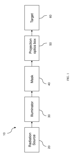
01 EUV lithography system design for miniaturization
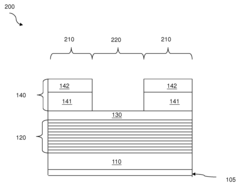
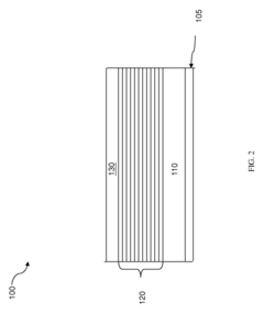
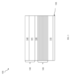
EUV lithography systems are designed specifically to achieve miniaturization in semiconductor manufacturing. These systems utilize extreme ultraviolet light with wavelengths around 13.5nm to pattern extremely small features on silicon wafers. The system design includes specialized optical components, mirrors, and illumination systems that enable the creation of nanoscale structures. Advanced EUV lithography systems can achieve feature sizes below 10nm, pushing the boundaries of semiconductor miniaturization.- EUV lithography system design for miniaturization: Advanced EUV lithography systems are designed specifically to achieve further miniaturization in semiconductor manufacturing. These systems incorporate specialized optical components, illumination systems, and precise positioning mechanisms to enable the creation of smaller feature sizes. The designs focus on optimizing the exposure process to achieve higher resolution patterns while maintaining manufacturing reliability at nanometer scales.
- Mask technology for EUV lithography: Specialized mask technologies are critical for EUV lithography miniaturization. These include reflective masks with multilayer coatings optimized for EUV wavelengths, advanced absorber materials, and novel mask structures that enhance pattern fidelity. Innovations in mask design help to overcome diffraction limits and enable the printing of increasingly smaller features while addressing challenges related to defects and pattern distortion at extreme scales.
- EUV source and illumination optimization: Innovations in EUV light sources and illumination systems are essential for miniaturization. These include high-power plasma sources, collector optics with enhanced reflectivity, and specialized illumination profiles that maximize resolution. Advanced techniques for controlling source power, stability, and spectral purity help to ensure consistent exposure quality while enabling smaller feature sizes and higher throughput in production environments.
- Computational lithography and correction techniques: Advanced computational methods enhance EUV lithography miniaturization capabilities. These include optical proximity correction, source mask optimization, and inverse lithography techniques that compensate for process limitations. Machine learning algorithms and simulation tools are employed to predict and correct for imaging artifacts, enabling the reliable production of smaller features beyond the nominal resolution limits of the optical system.
- Process integration and manufacturing solutions: Comprehensive process integration approaches enable practical implementation of EUV lithography for miniaturization in high-volume manufacturing. These solutions address challenges in resist chemistry, pattern transfer processes, and defect control. Novel multi-patterning techniques, specialized resist materials, and integrated metrology systems work together to enable reliable production of increasingly smaller semiconductor devices while maintaining yield and performance targets.
02 Photoresist and mask technology for EUV lithography
Specialized photoresist materials and mask technologies are crucial for EUV lithography miniaturization. EUV-specific photoresists are designed to be highly sensitive to extreme ultraviolet radiation while providing high resolution and low line edge roughness. Advanced mask technologies include reflective masks with multilayer coatings that enhance EUV reflection and reduce defects. These technologies work together to enable the precise pattern transfer necessary for creating increasingly smaller semiconductor features.Expand Specific Solutions03 Source and optics optimization for EUV lithography
EUV lithography miniaturization depends heavily on optimized light sources and optical systems. EUV sources typically use laser-produced plasma or discharge-produced plasma to generate the required 13.5nm wavelength light. Advanced optical systems employ multiple precision-engineered mirrors with multilayer coatings to collect, focus, and direct the EUV radiation. Continuous improvements in source power, stability, and optical efficiency are essential for achieving higher throughput and enabling further miniaturization of semiconductor devices.Expand Specific Solutions04 Contamination control and thermal management in EUV systems
Contamination control and thermal management are critical challenges in EUV lithography systems. Due to the high energy of EUV radiation, carbon contamination can occur on optical surfaces, reducing system performance over time. Advanced contamination control methods include hydrogen cleaning, specialized coatings, and environmental isolation. Thermal management systems are designed to handle the heat load generated by EUV sources and maintain the precise positioning of optical components, which is essential for achieving the nanometer-scale accuracy required for miniaturization.Expand Specific Solutions05 Computational lithography and process integration for EUV
Computational lithography techniques and process integration strategies are essential for maximizing EUV lithography capabilities. Advanced computational methods include optical proximity correction, source mask optimization, and inverse lithography technology, which enhance resolution and pattern fidelity. Process integration involves coordinating EUV lithography with other semiconductor manufacturing steps, such as etching and deposition, to achieve the desired device structures. These approaches enable semiconductor manufacturers to push the limits of miniaturization while maintaining yield and reliability.Expand Specific Solutions
Leading EUV Equipment Manufacturers and Chip Producers
EUV lithography represents a critical inflection point in semiconductor manufacturing, with the market currently in a growth phase characterized by increasing adoption despite high entry barriers. The global EUV market is expanding rapidly, projected to reach significant scale as miniaturization demands intensify. Technologically, industry leaders ASML Holding NV maintains dominant market position as the primary EUV equipment supplier, while semiconductor manufacturers like TSMC, Intel, and Samsung are at varying stages of implementation maturity. Research institutions including IMEC and universities collaborate with industry players to overcome technical challenges. The competitive landscape features established players investing heavily in EUV capabilities, with Asian manufacturers particularly aggressive in adoption to maintain technological leadership in advanced node production.
Taiwan Semiconductor Manufacturing Co., Ltd.
Technical Solution: TSMC has pioneered the implementation of EUV lithography in high-volume manufacturing, first deploying it at 7nm+ and extensively at 5nm nodes. Their approach integrates EUV into a hybrid lithography strategy, using it for critical layers while maintaining DUV for less demanding patterns. TSMC's EUV implementation includes proprietary resist chemistry optimization that balances sensitivity, resolution, and line edge roughness - achieving sub-20nm half-pitch resolution with single exposure[3]. Their manufacturing process incorporates specialized metrology systems for EUV-specific defect inspection and advanced computational lithography techniques to compensate for EUV-specific effects like mask 3D effects and stochastic variations. TSMC has developed custom pellicles compatible with EUV's high energy requirements and implemented sophisticated contamination control systems to maintain mask integrity. Their N3 (3nm) process node utilizes EUV for over 30 critical layers, enabling transistor densities exceeding 250 million transistors per square millimeter[4].
Strengths: Industry-leading implementation expertise with proven high-volume manufacturing capability; comprehensive process integration knowledge; advanced defect control and yield management systems for EUV. Weaknesses: Dependency on ASML as sole EUV equipment supplier; high capital expenditure requirements for maintaining technology leadership; challenges in managing stochastic defects at advanced nodes.
Intel Corp.
Technical Solution: Intel has developed a comprehensive EUV implementation strategy as part of its IDM 2.0 initiative. Their approach focuses on integrating EUV lithography into their process technology roadmap, beginning with Intel 4 (previously 7nm) and expanding significantly in Intel 3 and Intel 20A nodes. Intel's EUV implementation includes proprietary computational lithography techniques that optimize source-mask optimization (SMO) and optical proximity correction (OPC) specifically for their transistor architectures[5]. They've developed specialized resist materials in partnership with suppliers to enhance sensitivity while maintaining resolution requirements. Intel's approach includes advanced metrology systems specifically calibrated for EUV-specific defect types and pattern fidelity verification. Their EUV implementation strategy incorporates specialized design rules that maximize the benefits of EUV while minimizing its limitations, particularly for their unique gate-all-around transistor structures in future nodes. Intel has invested in developing specialized pellicles and reticle handling systems to extend mask lifetime and reduce defectivity[6].
Strengths: Vertical integration allowing customized EUV implementation for specific architecture needs; strong computational lithography capabilities; significant R&D resources. Weaknesses: Later adoption of EUV compared to competitors created technology gap; challenges in scaling production with new technology; complex transition managing both legacy and EUV-based manufacturing processes simultaneously.
Critical EUV Patents and Technical Innovations
Extreme ultraviolet lithography process and mask
PatentActiveUS9448491B2
Innovation
- A mask structure incorporating a reflective multilayer with a flare-suppressing absorption stack (FSAS) and a flare-suppressing-by-phase-shifting (FSbPhS) layer, which absorbs EUV light and induces destructive interference to suppress OOB radiation, specifically DUV flare, enhancing image contrast and lithography performance.
Method for extreme ultraviolet lithography
PatentInactiveUS6162577A
Innovation
- Development of photoresists that are more transparent to EUV radiation, specifically single-layer and bi-layer resist schemes, where the bi-layer resist includes a planarizing layer and a thin etch-resistant imaging layer, allowing for increased resolution and sensitivity, and using a reflective mask with a Schwarzschild camera for EUV lithography.
Supply Chain Dependencies for EUV Adoption
The successful implementation of EUV lithography technology depends on a complex and highly specialized global supply chain. ASML, the sole manufacturer of EUV lithography machines, relies on a network of over 5,000 suppliers across more than 60 countries. This intricate ecosystem creates significant dependencies and potential vulnerabilities that impact the broader semiconductor industry.
Critical components for EUV systems come from highly specialized suppliers. Carl Zeiss SMT in Germany produces the precision optical systems, including the crucial multi-layer mirrors that manipulate EUV light. Cymer, an ASML subsidiary in the United States, manufactures the sophisticated laser-produced plasma light sources. Japanese companies dominate the photomask and photoresist markets, with JSR Corporation and Tokyo Ohka Kogyo being key players in EUV-specific photoresist development.
The geographical concentration of these suppliers introduces strategic vulnerabilities. For instance, the Netherlands-based ASML's dependence on German optics, American light sources, and Japanese materials creates potential chokepoints. Trade restrictions or geopolitical tensions affecting any of these regions could disrupt the entire EUV supply chain, as evidenced by recent export controls targeting China's semiconductor industry.
Raw material constraints further complicate the supply chain landscape. EUV systems require specialized materials including high-purity neon gas for lasers, germanium for optical components, and rare earth elements for various precision parts. Many of these materials have limited sources globally, with some concentrated in politically sensitive regions, creating additional supply risks.
The high technical barriers to entry in the EUV supply chain have created natural monopolies in certain segments. ASML's exclusive position in EUV machine manufacturing exemplifies this concentration. Similarly, few companies can produce the ultra-flat, defect-free photomasks required for EUV lithography. This lack of supplier diversity increases dependency risks and potentially affects pricing dynamics.
The COVID-19 pandemic highlighted the fragility of the EUV supply chain, with disruptions causing delays in machine deliveries and semiconductor production. In response, major industry players have begun implementing supply chain resilience strategies. These include geographic diversification of suppliers, increased inventory of critical components, and in some cases, vertical integration to secure access to essential technologies and materials.
As EUV technology continues to advance toward High-NA EUV systems, supply chain dependencies will likely intensify. The even more specialized components required for these next-generation systems may further concentrate supplier power among a small number of highly capable companies, potentially exacerbating existing supply chain vulnerabilities in this critical technology area.
Environmental Impact of EUV Manufacturing Processes
The environmental footprint of Extreme Ultraviolet (EUV) lithography represents a significant consideration in semiconductor manufacturing. EUV systems consume substantial energy—approximately 1 megawatt per tool—primarily due to the complex process of generating EUV light. This process involves firing laser pulses at tin droplets to create plasma that emits the required 13.5nm wavelength radiation, resulting in considerable energy inefficiency with only about 1-2% of input power converted to usable EUV light.
Water usage presents another environmental challenge, with EUV systems requiring extensive cooling infrastructure. A single EUV lithography tool may consume thousands of gallons of ultra-pure water daily for temperature regulation and cleaning processes, contributing to water scarcity concerns in regions where semiconductor fabrication facilities operate.
Chemical consumption in EUV manufacturing introduces additional environmental considerations. The photoresist materials, developers, and cleaning agents used in the process often contain hazardous substances that require specialized handling and disposal protocols. While the industry has made progress in developing more environmentally friendly chemistries, the complex nature of EUV processes still necessitates the use of various specialized compounds.
Rare earth elements and specialized materials required for EUV components—particularly the highly engineered mirrors with multi-layer coatings—involve resource-intensive mining and processing operations. The environmental impact extends beyond the manufacturing facility to the global supply chain of these critical materials.
Waste management represents a significant operational challenge for EUV facilities. The process generates various waste streams including used photoresist materials, contaminated water, and worn components with specialized coatings that may contain hazardous substances requiring careful handling and disposal.
The semiconductor industry has recognized these environmental challenges and implemented various mitigation strategies. These include energy efficiency improvements, water recycling systems, and chemical recovery processes. Leading manufacturers have established ambitious sustainability goals, with companies like ASML, Intel, and TSMC investing in technologies to reduce the environmental footprint of EUV lithography.
As EUV technology continues to evolve, environmental considerations are increasingly integrated into the design and operation of next-generation systems. Research efforts focus on developing more energy-efficient light sources, environmentally friendly photoresist materials, and improved resource recovery methods, aiming to balance technological advancement with environmental responsibility.
Unlock deeper insights with Patsnap Eureka Quick Research — get a full tech report to explore trends and direct your research. Try now!
Generate Your Research Report Instantly with AI Agent
Supercharge your innovation with Patsnap Eureka AI Agent Platform!