Eureka AIR delivers breakthrough ideas for toughest innovation challenges, trusted by R&D personnel around the world.

Pixel structure of display device and pixel structure

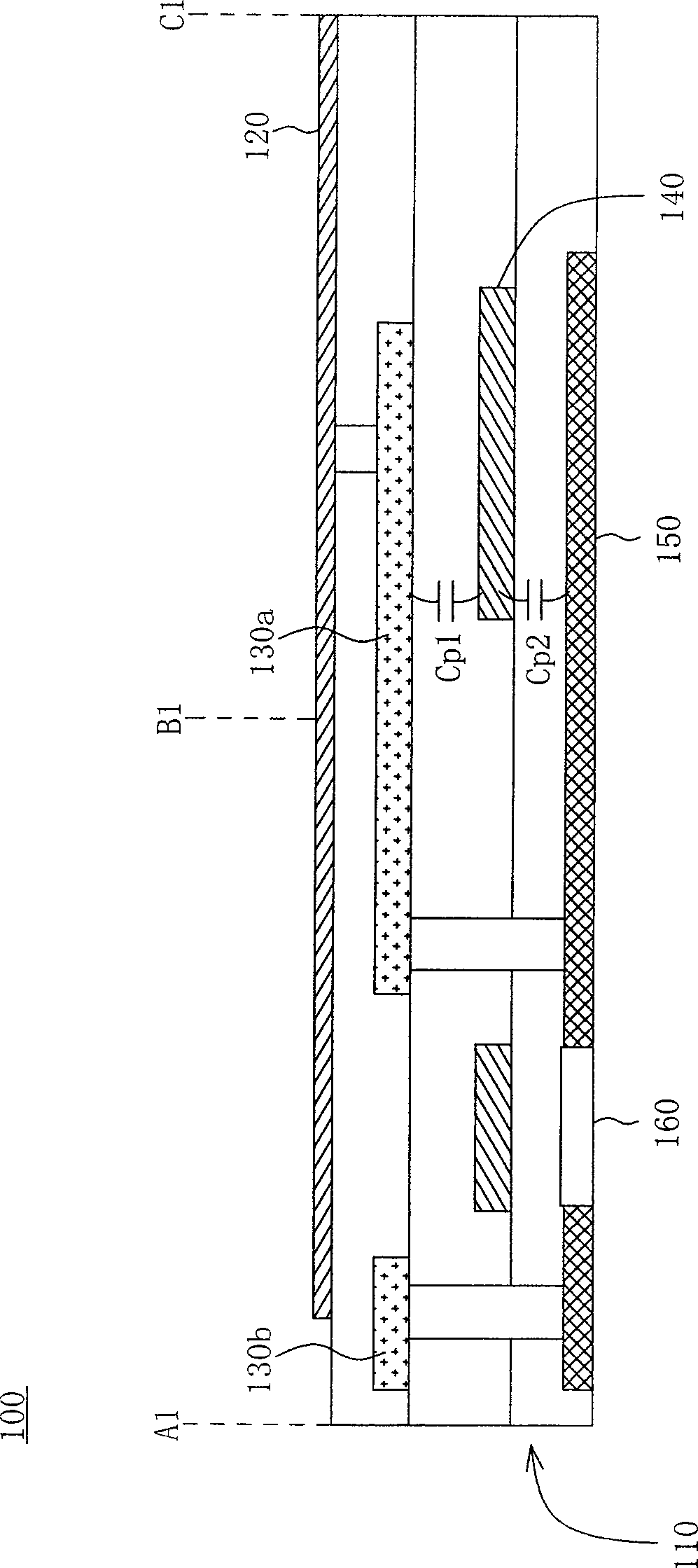
A technology of pixel structure and display device, applied in optics, instruments, electrical components, etc., can solve problems such as short circuit between metal plates 130a and 140

Active Publication Date: 2009-08-05
AU OPTRONICS CORP
View PDF7 Cites 5 Cited by
  • Summary
  • Abstract
  • Description
  • Claims
  • Application Information

AI Technical Summary

Problems solved by technology

[0005] However, due to process problems, metal particles (particles) remain between the metal plates 130a and 140, and the metal plates 130a and 140 are accidentally shorted.
Therefore, the storage capacitor Cp1 located between the metal plates 130a and 140 will disappear, resulting in a bright spot in the pixel 100

Method used


Image

  • Pixel structure of display device and pixel structure
  • Pixel structure of display device and pixel structure
  • Pixel structure of display device and pixel structure

Examples


Embodiment Construction

[0046] The following illustration and detailed description will make the spirit of the present invention clear. After understanding the embodiments of the present invention, those skilled in the art can make improvements and modifications to the present invention according to the embodiments of the present invention without departing from the spirit and scope of the present invention.

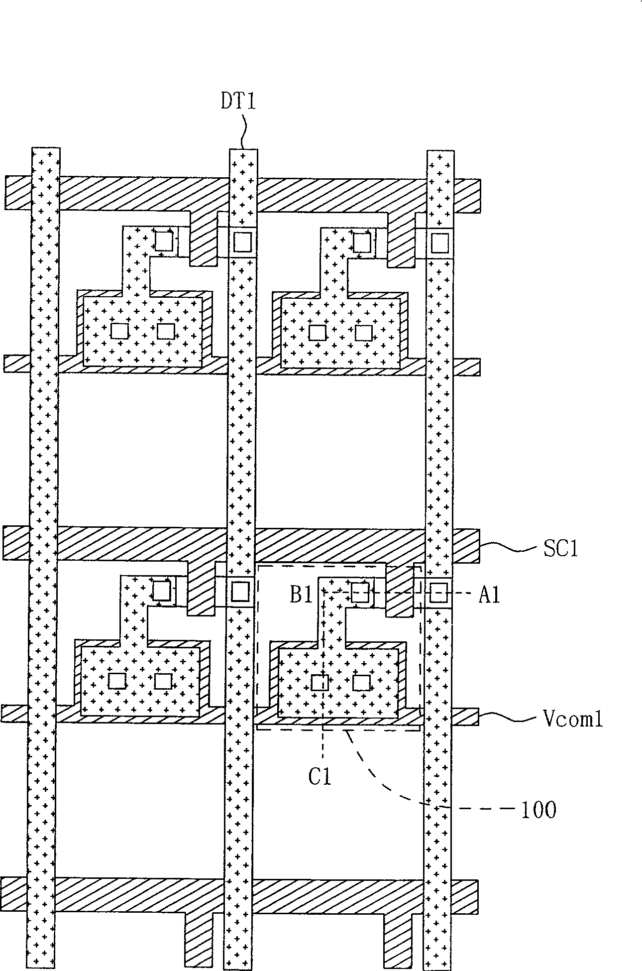
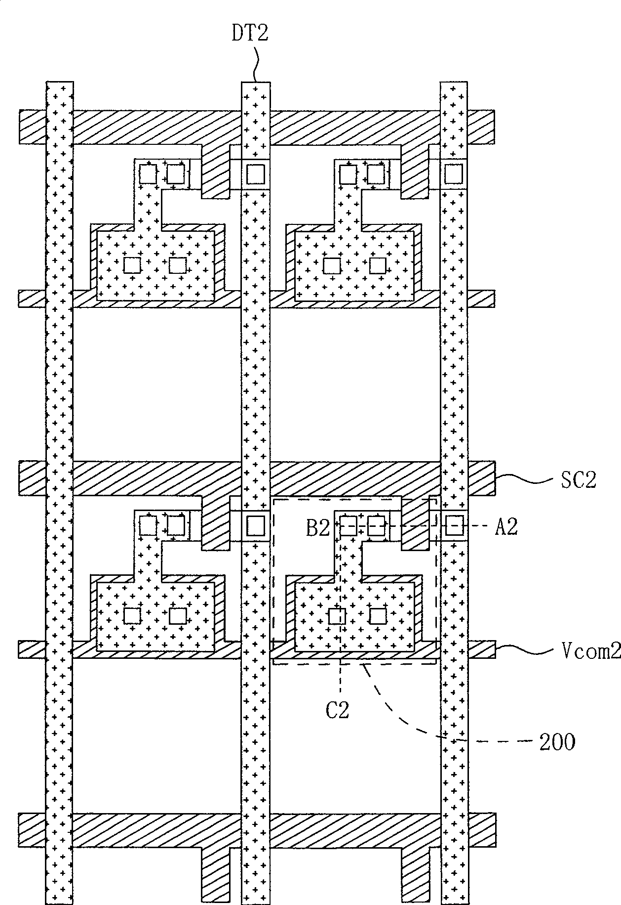
[0047] The pixel structure of the present invention includes two metal plates and a transistor. The two metal plates are electrically connected to each other. The gate of the transistor receives a scan signal. The drain of the transistor receives a data signal. The source of the transistor has two extensions. A storage capacitor is formed between the two extending portions and the two metal plates, wherein the two extending portions are planar structures.

[0048] Figure 2A A partial schematic diagram of a display panel formed from pixels having a pixel structure according to an embodimen...


PUM


Abstract

The invention discloses a pixel structure. The pixel structure includes two metal plates and a transistor. The two metal plates are electrically connected to each other. The gate of the transistor receives a scanning signal. The drain of the transistor receives a data signal. The source of the transistor has two extensions. A storage capacitor is formed between the two extension parts and the two metal plates, wherein the two extension parts are planar structures.

Description

technical field [0001] The present invention relates to a pixel structure of a display device, and more particularly, to a pixel structure in which a first metal plate and a second metal plate are coupled to form a storage capacitor. Background technique [0002] Figure 1A A partial schematic diagram showing a pixel structure in a conventional display panel. The pixel 100 is controlled by the scan line SC1, and receives the data signal transmitted by the data line DT1. Figure 1B A cross-sectional structural diagram of the pixel 100 is shown, wherein the cross-sectional structural diagram is Figure 1A Section in the direction of A1, B1 to C1. [0003] like Figure 1B As shown, the pixel structure of the pixel 100 is formed by an indium tin oxide (ITO) layer, a passivation layer, two metal plates, an interlayer dielectric (ILD), an oxide layer, and a polysilicon layer. The pixel 100 includes a transistor 110 and storage capacitors Cp1 and Cp2. The gate of the transistor...

Claims


Application Information

Patent Timeline
Patent Type & Authority Patents(China)
IPC IPC(8): H01L27/02H01L23/522G02F1/1368
Inventor 丁友信李雅君
Owner AU OPTRONICS CORP
Why Eureka
Eureka Blog
Learn More