

Image sensor with high fill factor pixels and method for forming an image sensor
A technology of image sensor and active area, which is applied in the fields of electrical solid-state devices, semiconductor devices, semiconductor/solid-state device manufacturing, etc., and can solve problems such as reducing image quality
- Summary
- Abstract
- Description
- Claims
- Application Information
AI Technical Summary
Problems solved by technology
Method used
Image

Examples
Embodiment Construction
[0088] The invention will now be described more particularly with reference to the accompanying drawings, in which preferred embodiments of the invention are shown. However, this invention may be embodied in different forms and should not be construed as limited to the embodiments set forth herein. Like reference numerals refer to like elements throughout the specification.
[0089] The invention will now be described in more detail with reference to the accompanying drawings, in which preferred embodiments of the invention are illustrated. However, this invention may be embodied in different forms and should not be construed as limited to the embodiments set forth herein. Throughout the specification, the same reference numerals refer to the same elements.
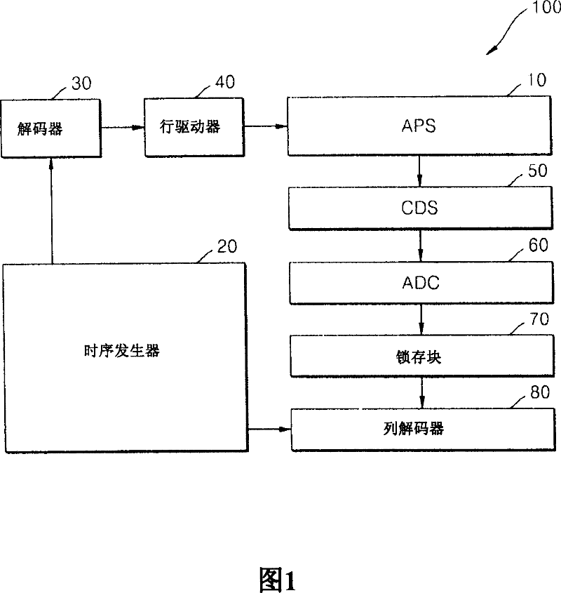
[0090] FIG. 1 is a block diagram of a CIS image sensor according to an embodiment of the present invention. Referring to FIG. 1 , a CIS image sensor 100 includes an active pixel sensor array (APS) 10, a timing generato...
PUM
 Abstract
Description
Claims
Application Information