
Manufacturing method for GaN-based LED (Light Emitting Diode) chip for increasing extraction efficiency
An LED chip and extraction efficiency technology, applied in electrical components, circuits, semiconductor devices, etc., can solve the problem of limited light extraction effect of GaN-based LEDs, and achieve the improvement of luminous optical power, increase the area of the light-emitting side, and increase the escape path. Effect
- Summary
- Abstract
- Description
- Claims
- Application Information
AI Technical Summary
Problems solved by technology
Method used
Image

Examples
Embodiment Construction
[0020] 1. Making LED chips:
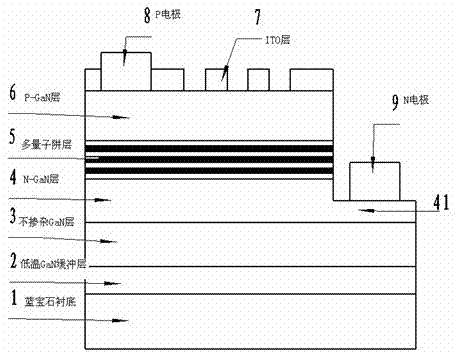
[0021] Step 1: Using metal-organic chemical vapor deposition (MOCVD), sequentially grow a 1 μm low-temperature GaN buffer layer 2, 1 μm undoped GaN layer 3, and 3 μm on a semiconductor substrate 1 made of sapphire, silicon, silicon carbide or metal materials N-GaN layer 4, 150nm multi-quantum well light-emitting layer 5 and 300nm P-GaN layer 6 form a GaN epitaxial wafer.
[0022] Step 2: Prepare the GaN epitaxial wafer for photolithographic patterning, use AZ4620 photoresist as a mask, and perform ICP (inductively coupled plasma) etching on one side of the GaN epitaxial wafer to remove P-GaN and quantum wells on one side And part of the N-GaN forms a mesa 41, and the etching depth of the mesa 41 is 700nm˜1500nm. ICP (Inductively Coupled Plasma) etching while using Cl 2 、BCl 3 and Ar 2 As an etching gas, where Cl 2 The flow rate is 30-100sccm, BCl 3 The flow rate is 5-20sccm, Ar 2 The flow rate is 5-25 sccm; the etching power is 300-700W; th...
PUM
 Abstract
Description
Claims
Application Information