A method and device for preparing an optical film with a concave structure on the surface

An optical film and recessed structure technology, which is applied to optical components, household appliances, other household appliances, etc., can solve the problems such as the inability to meet the special use needs of optical films, the single macroscopic structure of the optical film surface, and the complex preparation process, and improve the surface of the optical film. The effect of functional properties, technical means and simple operation

CN104647770BActive Publication Date: 2017-10-20SOUTH CHINA UNIV OF TECH
7 Cites 0 Cited by

Patent Information

Authority / Receiving Office
CN · China
Patent Type
Patents(China)
Current Assignee / Owner
Publication Date
2017-10-20

Smart Images

  • Figure 1
    Figure 1
  • Figure 2
    Figure 2
  • Figure 3
    Figure 3
Patent Text Reader

Abstract

The invention discloses a method and device for preparing an optical film with a concave structure on the surface, comprising a mold body, edge-holding mechanisms arranged on both sides of the mold body for tightening the edge of the film template, and thimbles arrayed in the mold body Channel, the thimble channel is provided with a thimble, and the thimble can move up and down on the upper surface of the mold body and the thimble channel through the jacking mechanism; the jacking mechanism is used to control the height of the thimble on the upper surface of the mold body; the shape and distribution of the thimble By designing, optical films with one or more shapes and highly combined concave structures on the surface can be obtained, thereby improving the corresponding surface functional properties of the film. In this method, the shape, height and distribution of the thimble are adjustable, and the adaptability is strong. It has the advantages of simple operation, strong flexibility, cost saving, and good sample consistency.
Need to check novelty before this filing date? Find Prior Art

Description

technical field

[0001] The invention relates to the preparation of an optical thin film, in particular to a method and a device for preparing an optical thin film with a concave structure on the surface. Background technique

[0002] Thin film is a thin layer of solid material grown on the surface of the substrate by a specific preparation method. It has the characteristics of large surface energy level, strong adhesion and changing optical properties. It is widely used in electronic appliances, machinery, printing and other industries. The preparation methods of thin films can be divided into physical vapor deposition method, chemical vapor deposition method, sol-gel method and electrodeposition method according to broad categories. Among them, the spin-coating method in the sol-gel method is a high-quality film preparation method. The substrate with a micro-nano structure on the surface can be used as a matrix, and a micro-scale functional structure film with uniform thick...

Examples

Embodiment

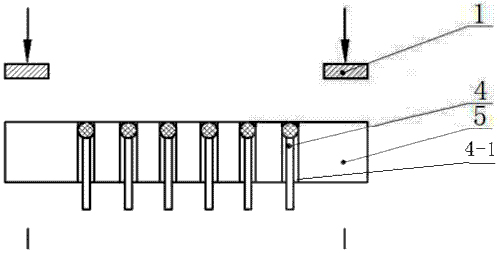
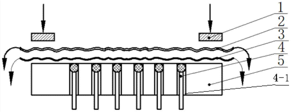
[0034] like figure 1 shown. The present invention is a device used in the preparation of an optical film with a concave structure on the surface. The device includes a mold body 5, a crimping mechanism 1 arranged on both sides of the mold body 5 for tightening the edge of the film template 2, and an array distributed on the mold The thimble channel 4-1 in the body 5, the thimble channel 4-1 is provided with a thimble 4, and the thimble 4 can move up and down on the upper surface of the mold body 5 and the thimble channel 4-1 through the jacking mechanism (using hydraulic pressure); The lifting mechanism is used to control the height of the ejector pin 4 on the upper surface of the mold body 5;

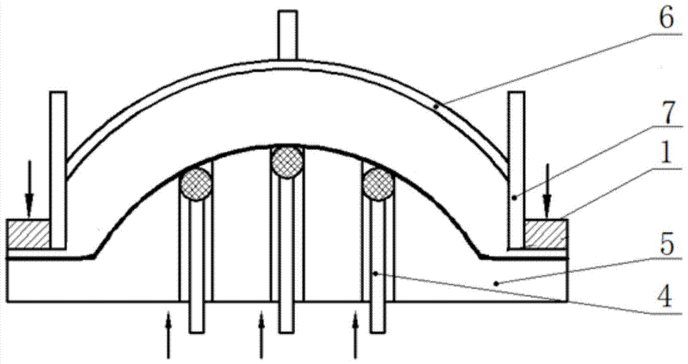
[0035] like Figure 5 mentioned. The mold also includes an auxiliary pressing plate 6, which is used to squeeze the silica gel 8 from top to bottom during the use of the mould. An auxiliary dam 7 for enclosing the colloid 8 is added on the inner side of the crimping mechanism 1 . ...