Substrate, display panel and display device

A display panel and substrate technology, applied in the direction of instruments, nonlinear optics, optics, etc., can solve problems such as display abnormality, liquid crystal pollution on the edge of the display area, and affect the display effect of the liquid crystal display, so as to ensure the display effect and avoid pollution.

Inactive Publication Date: 2016-10-12
BOE TECH GRP CO LTD +1
View PDF5 Cites 8 Cited by
  • Summary
  • Abstract
  • Description
  • Claims
  • Application Information

AI Technical Summary

Problems solved by technology

If the diffusion speed of the liquid crystal is too fast, contacting it before the sealant is completely cured will cause the liquid crystal at the edge of the display area to be polluted, and the liquid crystal cannot be deflected normally, resulting in abnormal display; if the diffusion speed of the liquid crystal is too slow, the liquid crystal in the non-disp

Method used


Image

  • Substrate, display panel and display device
  • Substrate, display panel and display device
  • Substrate, display panel and display device

Examples


Embodiment 1

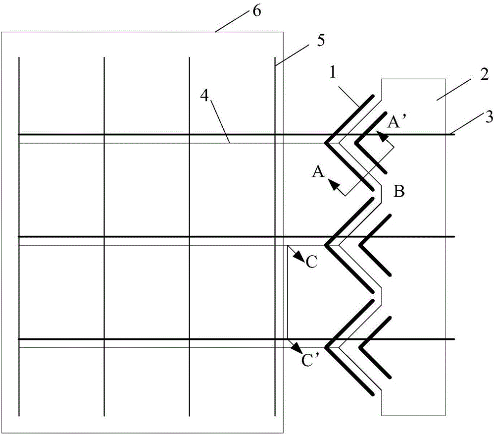
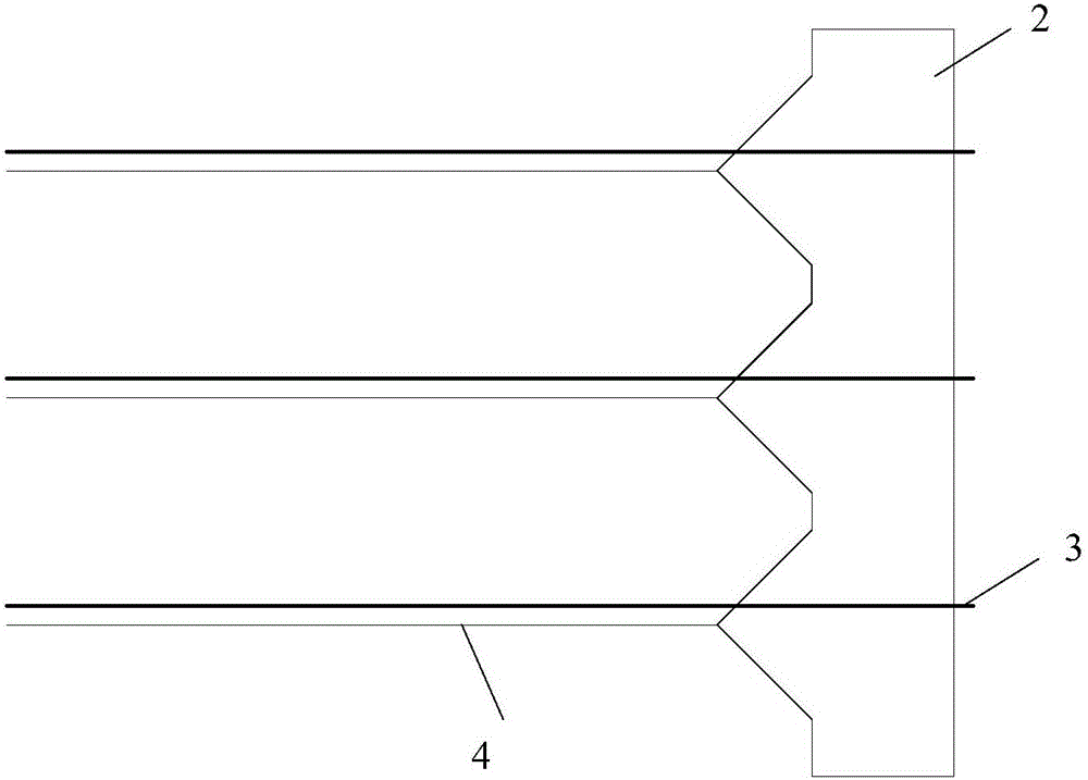
[0033] This embodiment provides a substrate. The substrate includes a display area and a non-display area located around the display area. A plurality of spacers arranged at intervals are arranged in the non-display area of ​​the substrate near the display area.

[0034] In this embodiment, a plurality of spacers arranged at intervals are arranged near the non-display area of ​​the substrate to the position of the display area, and the cooperation of the plurality of spacers can effectively block the diffusion of liquid crystal and prevent the liquid crystal in the display area from sealing the frame. The contact of the glue phase prevents the liquid crystal from being polluted, and can better prevent bubbles from moving from the non-display area to the display area, so as to ensure the display effect of the display device.

[0035] Further, the spacer is a linear spacer, and the orthographic projection of the linear spacer on the substrate is elongated. Unlike the existing col...

Embodiment 2

[0044] An embodiment of the present invention also provides a display panel, including the substrate as described above, the substrate is a color filter substrate, and the display panel further includes an array substrate arranged in a box with the substrate.

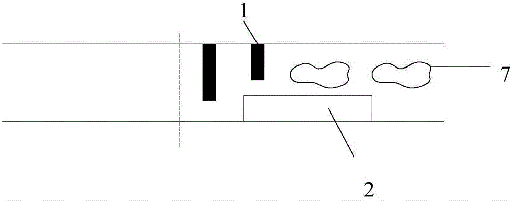
[0045] In a specific embodiment, the array substrate is provided with a conductive pattern connected to a common voltage, and in the same group of linear spacers, the orthographic projection of at least one linear spacer on the array substrate falls into the orthographic projection of the conductive pattern on the array substrate. The combination of the linear spacer and the conductive pattern can better prevent the liquid crystal from entering the non-display area, and prevent air bubbles from entering the display area.

[0046] Further, the same group of linear spacers includes a first linear spacer and a second linear spacer, and the orthographic projection of the second linear spacer on the array substrate falls into t...

Embodiment 3

[0050] This embodiment also provides a display device, including the above-mentioned substrate. The display device can be any product or component with display function such as LCD TV, liquid crystal display, digital photo frame, mobile phone, tablet computer, etc., wherein the display device also includes a flexible circuit board, a printed circuit board and a backplane.


PUM


Abstract

The invention provides a substrate, a display panel and a display device, and belongs to the technical field of display. The substrate comprises a display area and a non-display area located on the periphery of the display area. Multiple spacers are arranged at the position, close to the display area, of the non-display area of the substrate at intervals. According to the technical scheme, the display effect of the display device can be improved.

Description

technical field [0001] The present invention relates to the field of display technology, in particular to a substrate, a display panel and a display device. Background technique [0002] At present, as an important part of the information industry, display devices are accelerating their flattening process. The world has entered the era of "information revolution". Display technology and display devices occupy a very important position in the development of information technology. Daily life and work provide a lot of information. [0003] The manufacturing process of liquid crystal displays includes: array substrate preparation process, color film substrate preparation process and liquid crystal cell preparation process. The liquid crystal cell preparation process includes applying sealant on the periphery of the array substrate. It is the process of pouring liquid crystals, aligning the prepared color filter substrate and array substrate precisely in units of unit pixels, ...

Claims


Application Information

Patent Timeline
IPC IPC(8): G02F1/1339
CPCG02F1/13394G02F1/1339G02F1/13396G02F1/136286
Inventor 李洋刘华封宾孙鹏石虎兆
Owner BOE TECH GRP CO LTD
Why Eureka
Try Eureka