Array substrate, production method thereof, display panel, and display device

A technology for array substrates and display devices, which is applied in semiconductor/solid-state device manufacturing, optics, instruments, etc., and can solve the problems of light leakage and serious illumination of thin film transistors

Active Publication Date: 2017-10-17
XIAMEN TIANMA MICRO ELECTRONICS
View PDF5 Cites 19 Cited by
  • Summary
  • Abstract
  • Description
  • Claims
  • Application Information

AI Technical Summary

Problems solved by technology

[0005] In view of this, the embodiments of the present invention provide an array substrate and its manufacturing method, a display panel, and a display device, which are used to solve the

Method used


Image

  • Array substrate, production method thereof, display panel, and display device
  • Array substrate, production method thereof, display panel, and display device
  • Array substrate, production method thereof, display panel, and display device

Examples


Embodiment Construction

[0033] In order to better understand the technical solutions of the present invention, the embodiments of the present invention will be described in detail below in conjunction with the accompanying drawings.

[0034] It should be clear that the described embodiments are only some of the embodiments of the present invention, not all of them. Based on the embodiments of the present invention, all other embodiments obtained by persons of ordinary skill in the art without creative efforts fall within the protection scope of the present invention.

[0035] It should be noted that, in the case of no conflict, the embodiments of the present invention and the features in the embodiments can be combined with each other. The present application will be described in detail below with reference to the accompanying drawings and embodiments.

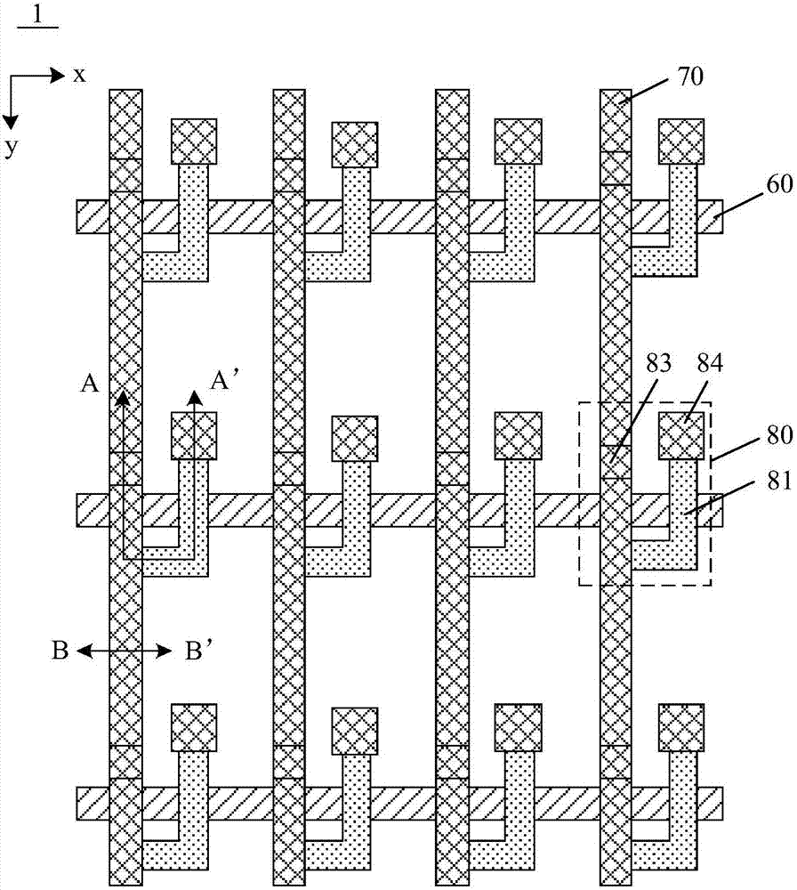
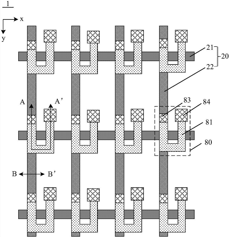
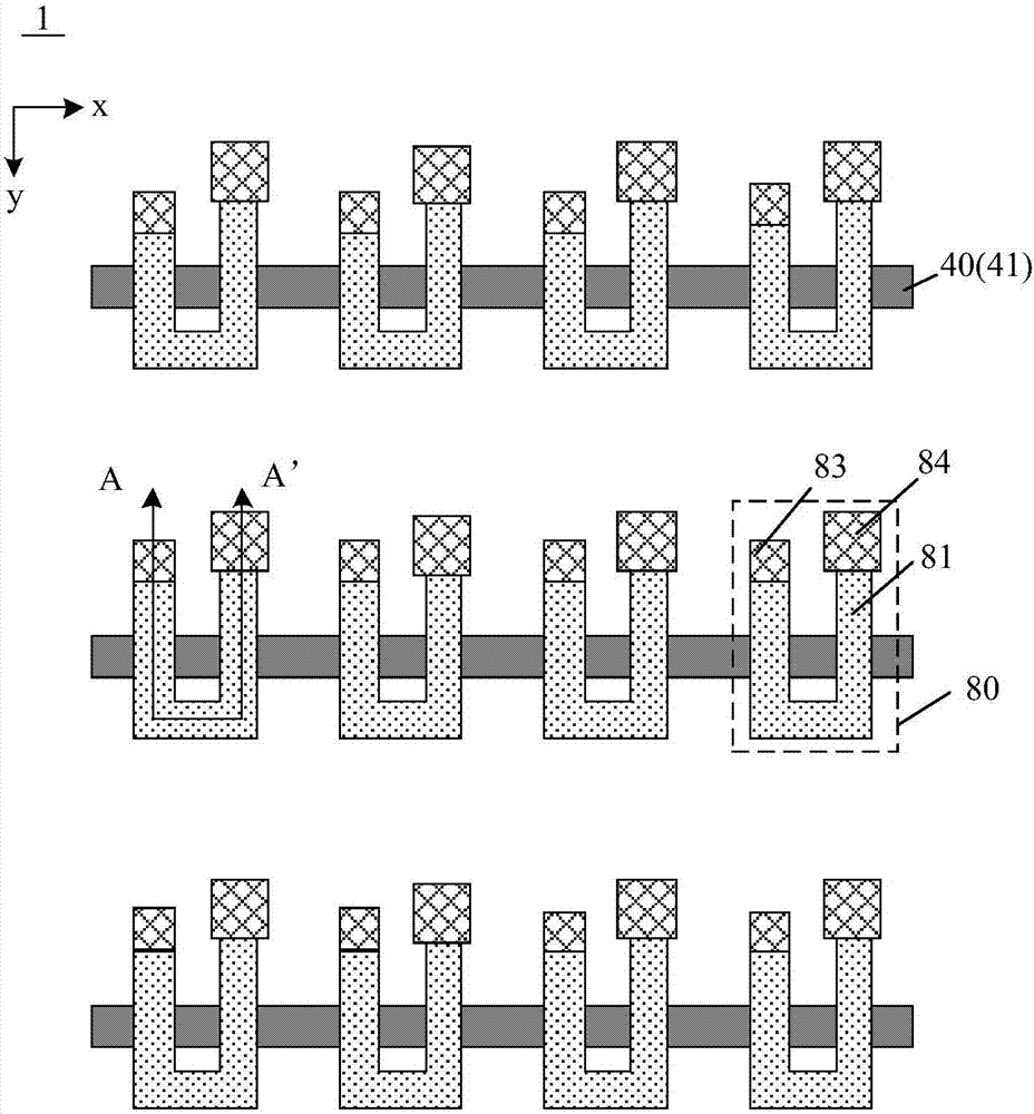
[0036] An embodiment of the present invention provides an array substrate, such as figure 1 , figure 2 , image 3 and Figure 4 as shown, Fi...


PUM

PropertyMeasurementUnit
Thicknessaaaaaaaaaa
Thicknessaaaaaaaaaa
Thicknessaaaaaaaaaa

Abstract

The invention provides an array substrate, a production method thereof, a display panel, and a display device, and relates to the display technology field. The array substrate comprises a substrate; an auxiliary shade layer, an insulation layer, a main shade layer, and a buffer layer, which are sequentially arranged in a direction away from the substrate. A plurality of grid lines and a plurality of data lines are used to form a plurality of pixel areas in a limited way, and thin film transistors are disposed in the pixel areas. The auxiliary shade layer comprises a plurality of first auxiliary shade parts, and the main shade layer comprises a plurality of main shade parts. The orthogonal projection of the channel areas of the active layers of the thin film transistors on the array substrate is disposed in the orthogonal projection of the main shade parts on the array substrate, and the orthogonal projection of the channel areas of the active layers of the thin film transistors on the array substrate is disposed in the orthogonal projection of the first auxiliary shade parts on the array substrate. By adopting the technical scheme provided by the invention, intensities of light irradiated on the channel areas of the active layers of the thin film transistors are reduced, and the light leakage flows of the thin film transistors are reduced.

Description

【Technical field】 [0001] The present invention relates to the field of display technology, in particular to an array substrate and a manufacturing method thereof, a display panel and a display device. 【Background technique】 [0002] Generally, a display device includes a display panel and a backlight module, wherein the display panel is used to display images, but the display panel itself cannot emit light, and the backlight module needs to provide light for it. [0003] The display panel includes an array substrate, a color filter substrate, and a liquid crystal layer located between the array substrate and the color filter substrate, wherein the array substrate is arranged facing the backlight module, and a plurality of thin film transistors are arranged on the array substrate, and the active layer of the thin film transistor The channel area is sensitive to light. In the prior art, a light-shielding layer is provided on the side of the active layer facing the backlight mo...

Claims


Application Information

Patent Timeline
IPC IPC(8): H01L27/12H01L21/77G02F1/1362
CPCG02F1/136209H01L27/1214H01L27/1296
Inventor 钟彩娇林友道周婷沈柏平
Owner XIAMEN TIANMA MICRO ELECTRONICS
Why Eureka
Try Eureka