Gate driving circuit, manufacturing method thereof, and driving method

A technology of a gate drive circuit and a drive method, which is applied in the fields of a gate drive circuit and its manufacturing method, a display device, an array substrate, and a drive method, and can solve problems such as difficulty in uniform display brightness of pixels on a special-shaped display screen

Active Publication Date: 2020-06-02
BOE TECH GRP CO LTD
View PDF12 Cites 0 Cited by
  • Summary
  • Abstract
  • Description
  • Claims
  • Application Information

AI Technical Summary

Problems solved by technology

[0004] The purpose of the embodiments of the present invention is to provide a gate driving circuit and its manufacturing method, driving method, array substrate, and display device, which are used to solve the problem that the pixel display brightness of each row of a special-shaped display screen is difficult to be consistent

Method used


Image

  • Gate driving circuit, manufacturing method thereof, and driving method
  • Gate driving circuit, manufacturing method thereof, and driving method
  • Gate driving circuit, manufacturing method thereof, and driving method

Examples


Embodiment Construction

[0023] In order to further illustrate the gate driving circuit provided by the embodiments of the present invention, its manufacturing method, driving method, array substrate, and display device, a detailed description will be given below in conjunction with the accompanying drawings.

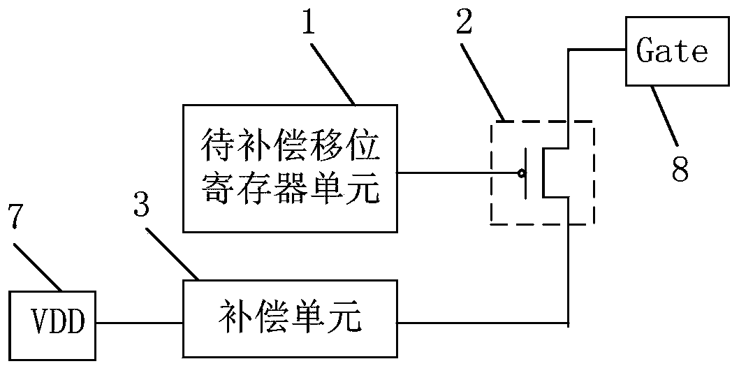
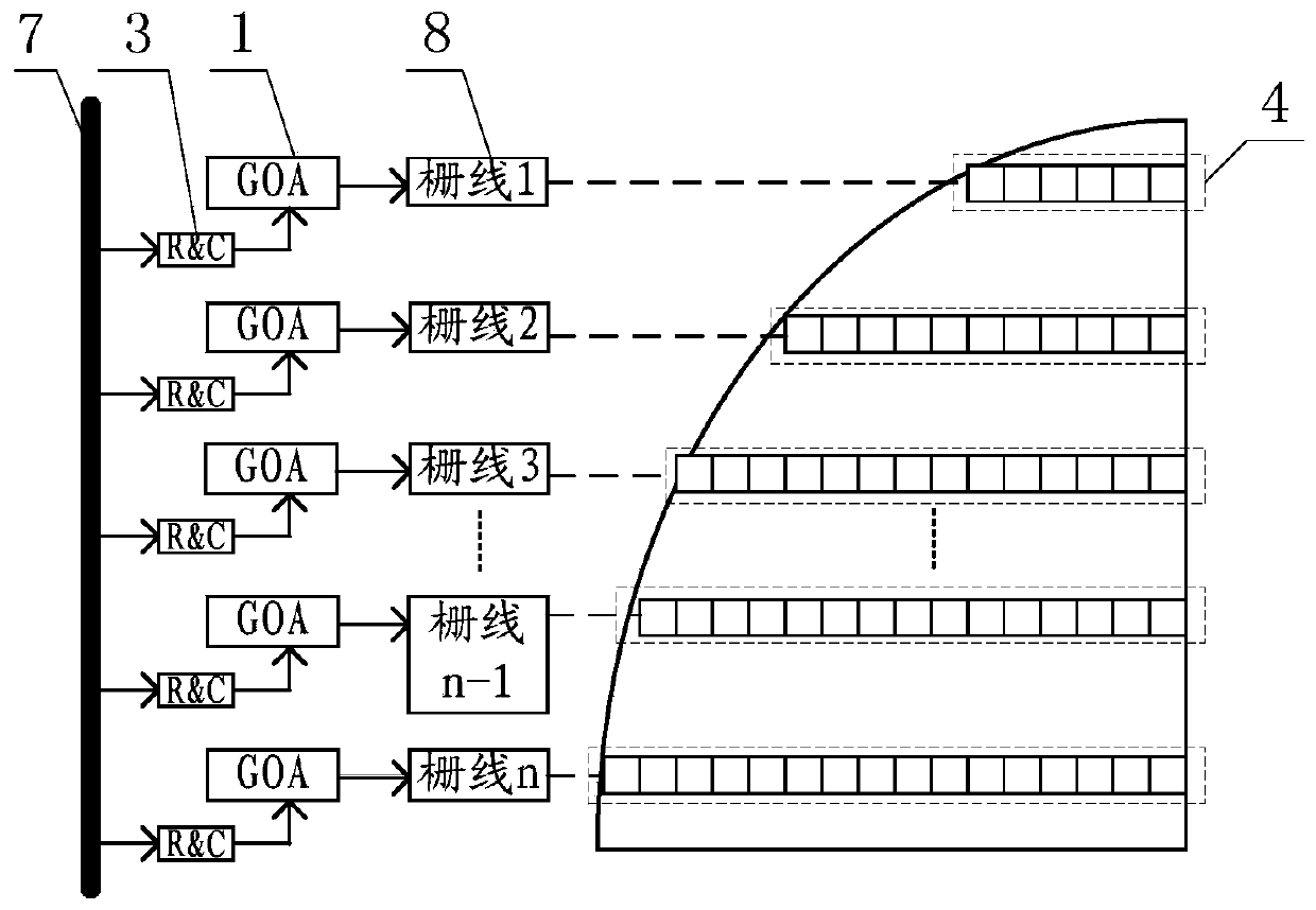
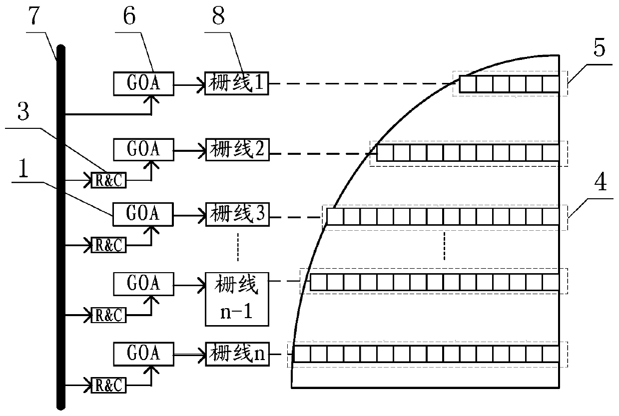
[0024] For a special-shaped display screen, the number of pixel units arranged in each row of pixels is likely to be different. If the number of pixel units set in each row of pixels of the special-shaped display screen is different, then the gate parasitic generated by each row of pixels will be approximately proportional to the number of pixel units in the corresponding row of pixels, so that each The gate parasitics generated by rows of pixels are also different, and the gate parasitics include gate parasitic capacitance and gate parasitic resistance; and because the structures of the shift register units at all levels in the gate drive circuit are the same, that is, each level of shift The ...


PUM


Abstract

The embodiments of the present disclosure disclose a gate driving circuit. The gate driving circuit includes at least one stage of shift register unit to be compensated, wherein a driving terminal of each stage of shift register unit to be compensated is connected to a gate line of a corresponding row of pixels to be compensated, and at least one stage of parasitics compensation circuit, wherein each stage of parasitics compensation circuit is connected in series between a power supply line and a driving terminal of a corresponding shift register unit to be compensated. Each stage of parasitics compensation circuit is configured to compensate a driving terminal of a corresponding shift register unit to be compensated for parasitic capacitance and / or parasitic resistance, so that respective stages of shift register units to be compensated have the same driving load.

Description

technical field [0001] The present invention relates to the field of display technology, in particular to a gate driving circuit, a manufacturing method thereof, a driving method, an array substrate, and a display device. Background technique [0002] With the development of display technology, the Organic Light Emitting Diode (Organic Light Emitting Diode) display device is recognized by the industry as one of the most promising display devices due to its advantages of thinness, bright color, and high contrast. [0003] At present, in order to meet the diverse needs of users, the shapes of the display screens in OLED display devices are also becoming more and more diverse, and some special-shaped display screens such as circular, elliptical, or polygonal shapes have appeared. However, for a special-shaped display screen, the number of pixel units set in each row of pixels is likely to be different, so that when the gate drive circuit is used to drive the row pixels of diffe...

Claims


Application Information

Patent Timeline
Patent Type & Authority Patents(China)
IPC IPC(8): G09G3/3208G11C19/28
CPCG09G3/3208G09G2310/0286G09G2320/0233G11C19/28G09G3/3266
Inventor 朱健超刘利宾
Owner BOE TECH GRP CO LTD
Why Eureka
Try Eureka