AI technical title is built by Patsnap AI team. It summarizes the technical point description of the patent document.
A technology of display panel and sub-panel, applied in the field of display panel and display device, can solve the problems of unsatisfactory display effect of dual-box display panel and the like
Active Publication Date: 2019-11-01
BOE TECH GRP CO LTD
View PDF5 Cites 6 Cited by
Summary
Abstract
Description
Claims
Application Information
AI Technical Summary
This helps you quickly interpret patents by identifying the three key elements:
Problems solved by technology
Method used
Benefits of technology
Problems solved by technology
[0004] The present invention at least partly solves the problem of the unsatisfactory display effect of the existing double-box display panel, and provides a display panel and a display device that can improve the display effect
Method used
Image
Click on the blue label to locate the original text in one second.
Reading with bidirectional positioning of images and text.
Examples
Embodiment 1
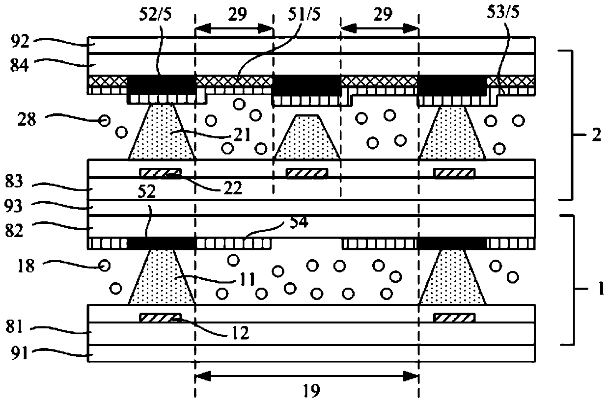
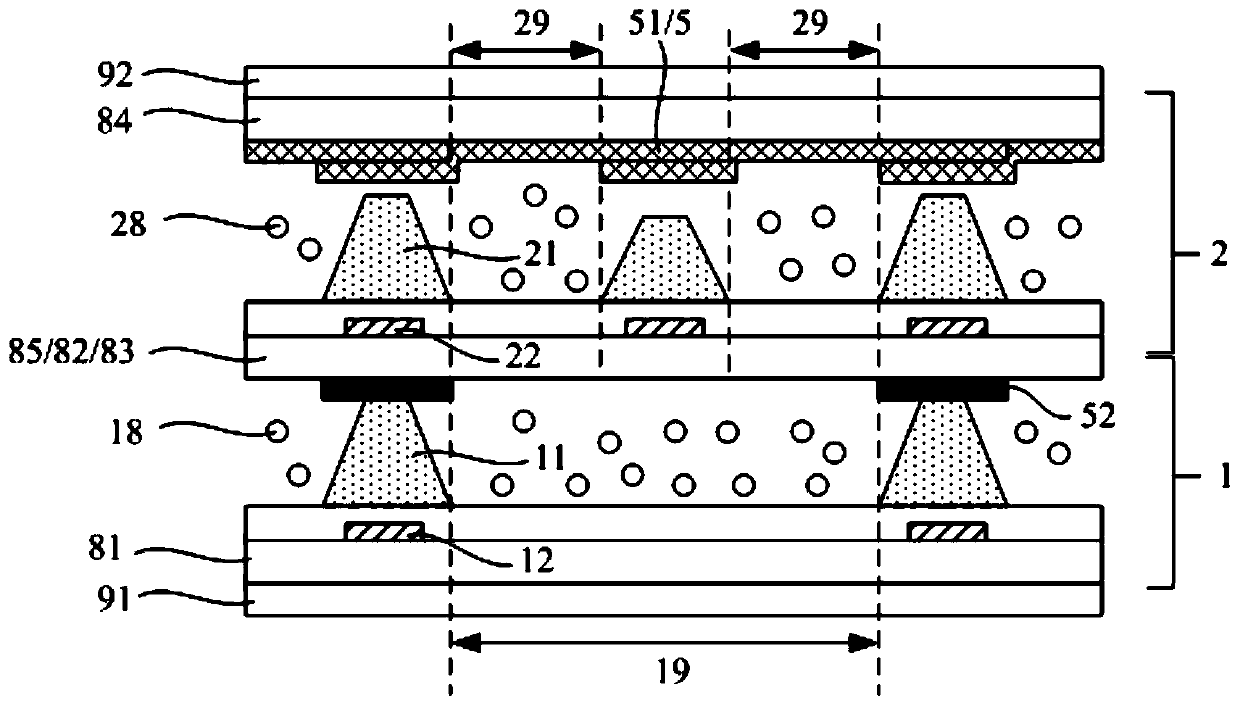
[0049] refer to Figure 1 to Figure 3 , an embodiment of the present invention provides a display panel, which includes:
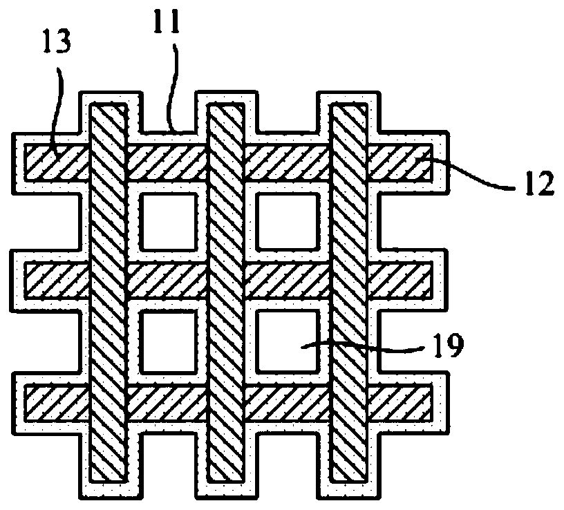
[0050] The first sub-panel 1 includes a first substrate 81 and a second substrate 82 opposite to each other, and a first medium 18 and a first spacer wall 11 disposed between the first substrate 81 and the second substrate 82; The sub-panel 1 has a plurality of filter pixels 19 arranged at intervals, and the filter pixels 19 are used to generate a driving electric field in the first medium 18 to control its own light transmittance; the first spacer wall 11 is black, along the filter pixels 19, and the dielectric coefficient is greater than the dielectric coefficient of the first medium 18;
[0051] Set on the light-emitting side of the first sub-panel 1 ( figure 1 , figure 2 Take the upper side as an example) the second sub-panel 2, which includes the opposite third substrate 83, the fourth substrate 84, and the second medium 28 and the second spacer a...
Embodiment 2
[0100] An embodiment of the present invention provides a method for manufacturing the above-mentioned display panel, which includes the step of forming each structure in the above two sub-panels.
[0101] For example, a method for preparing the above-mentioned display panel may specifically include:
[0102] S2001. Form a gate (GATE) and a first gate line on a first substrate through a patterning process.
[0103] S2002, forming a gate insulating layer (GI) on the first substrate.
[0104] S2003, forming an active layer (ACT) on the first substrate through a patterning process.
[0105] S2004, forming an interlayer insulating layer on the first substrate through a patterning process.
[0106] S2005. Form a source electrode, a drain electrode, and a first data line (DATA) on the first substrate through a patterning process.
[0107] S2006, forming a passivation layer (PVX) on the first substrate through a patterning process.
[0108] S2007, forming a first pixel electrode (...
Embodiment 3
[0140] An embodiment of the present invention provides a display device, which includes:
[0141] The above display panel:
[0142] The backlight installed on the light-incident side of the display panel.
PUM
Abstract
The invention provides a display panel and a display device, belonging to the technical field of display, and aiming to at least partially solve the problem that the display effect of an existing dual-box display panel is unsatisfactory. The display panel of the embodiment of the invention includes: a first sub-panel and a second sub-panel, wherein the first sub-panel includes a first medium and afirst spacer wall that are arranged between a first substrate and a second substrate; the first sub-panel is provided with a plurality of spaced filter pixels; the first spacer wall is black and is distributed along the intervals of the filter pixels, and the dielectric coefficient of the first spacer wall is greater than the dielectric coefficient of the first medium; the second sub-panel is arranged on the light-emitting side of the first sub-panel, the second sub-panel includes a second medium and a second spacer wall that are arranged between a third substrate and a fourth substrate, andthe second sub-panel is provided with a plurality of display pixels arranged at intervals; the second spacer wall is black and is distributed along the intervals of the display pixels, and the dielectric coefficient of the second spacer wall is greater than the dielectric coefficient of the second medium; the second substrate is located on the light-emitting side of the first sub-panel, and the third substrate is located on the light-incoming side of the second sub-panel.
Description
technical field [0001] The invention belongs to the field of display technology, and in particular relates to a display panel and a display device. Background technique [0002] In order to improve the contrast of the LCD panel, two LCD panels can be stacked together to form a double-cell (double-cell) display panel. One of the LCD panels is used to initially filter the light from the backlight, and the other LCD panel is used for the backlight. The light is finally filtered to enable the display. [0003] Because the light has been filtered twice, the contrast ratio of the dual-box display panel is very high, comparable to that of an organic light-emitting diode display panel (OLED), which can reach more than 150,000. However, the display effect of the dual box display panel is still not ideal. Contents of the invention [0004] The present invention at least partly solves the problem of the unsatisfactory display effect of the existing double-box display panel, and pro...
Claims
Application Information
Patent Timeline
Application Date:The date an application was filed.
Publication Date:The date a patent or application was officially published.
First Publication Date:The earliest publication date of a patent with the same application number.
Issue Date:Publication date of the patent grant document.
PCT Entry Date:The Entry date of PCT National Phase.
Estimated Expiry Date:The statutory expiry date of a patent right according to the Patent Law, and it is the longest term of protection that the patent right can achieve without the termination of the patent right due to other reasons(Term extension factor has been taken into account ).
Invalid Date:Actual expiry date is based on effective date or publication date of legal transaction data of invalid patent.

