Circuit board schematic diagram design method and device, electronic equipment and storage medium

A design method and schematic diagram technology, applied in the field of data processing, can solve problems that affect the realization of circuit board functions, are prone to errors, and take a long time

Pending Publication Date: 2020-07-03
INSPUR BUSINESS MACHINE CO LTD
View PDF4 Cites 3 Cited by
  • Summary
  • Abstract
  • Description
  • Claims
  • Application Information

AI Technical Summary

Problems solved by technology

Since the design process of the existing circuit board schematic diagram requires manual implementation by relevant technical personnel, the current ...

Method used


Image

  • Circuit board schematic diagram design method and device, electronic equipment and storage medium
  • Circuit board schematic diagram design method and device, electronic equipment and storage medium
  • Circuit board schematic diagram design method and device, electronic equipment and storage medium

Examples


Embodiment Construction

[0036] In order to make the purpose, technical solutions and advantages of the embodiments of the present invention clearer, the technical solutions in the embodiments of the present invention will be clearly and completely described below in conjunction with the drawings in the embodiments of the present invention. Obviously, the described embodiments It is a part of embodiments of the present invention, but not all embodiments. Based on the embodiments of the present invention, all other embodiments obtained by persons of ordinary skill in the art without making creative efforts belong to the protection scope of the present invention.

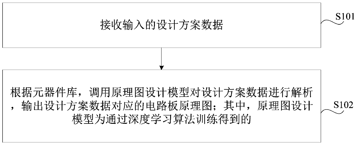
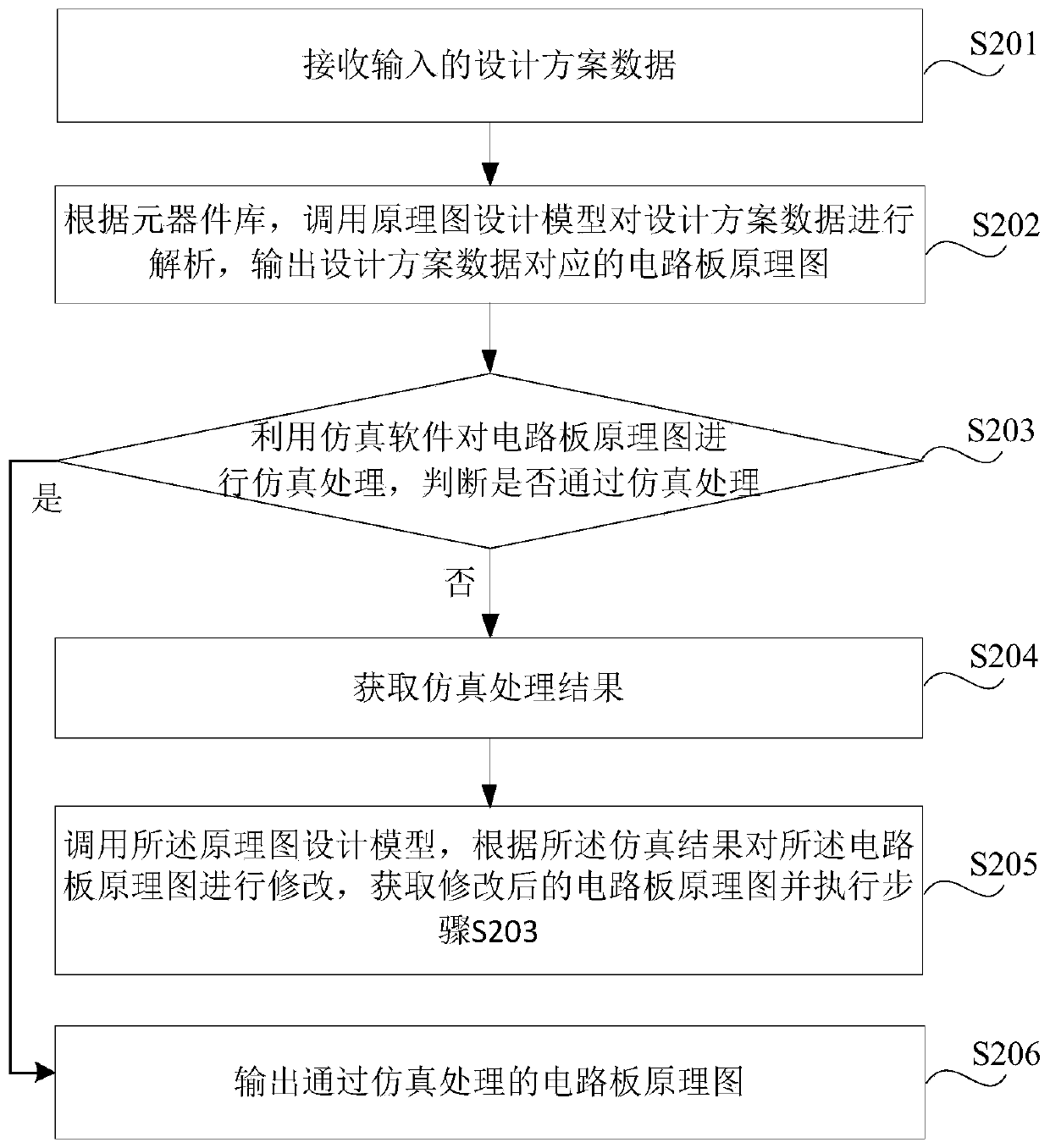
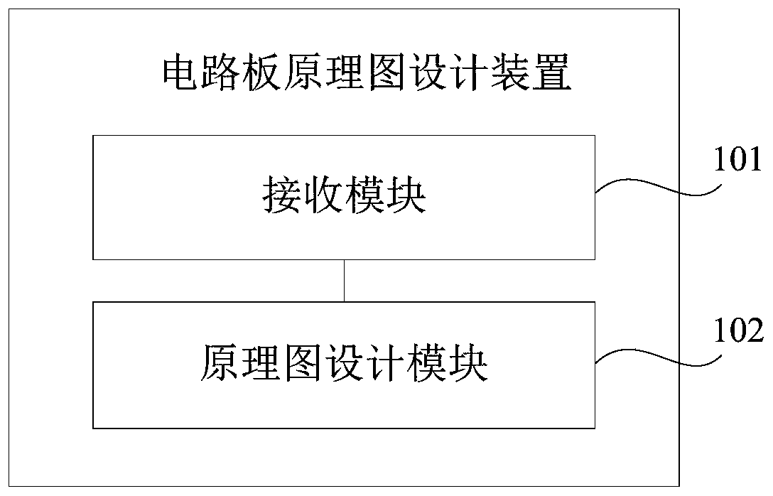
[0037] At present, the design of the schematic diagram of the circuit board is done manually according to the design data of the components used on the circuit board, and the design software of the schematic diagram of the circuit board is used to realize the design of the schematic diagram of the circuit board. It requires professional techn...


PUM


Abstract

The invention provides a circuit board schematic diagram design method and device, electronic equipment and a storage medium. The method comprises the steps of receiving input design scheme data; according to the component library, calling a schematic diagram design model to analyze the design scheme data, and outputting a circuit board schematic diagram corresponding to the design scheme data; wherein the schematic diagram design model is obtained by training through a deep learning algorithm; the method comprises the following steps: automatically analyzing received design scheme data by utilizing a schematic diagram design model obtained by training a deep learning algorithm, and automatically obtaining a circuit board schematic diagram corresponding to the design scheme data input by auser according to related component design data obtained from a component library; the automatic design of the schematic diagram of the circuit board is realized, the design efficiency of the schematic diagram of the circuit board is improved, and the whole design process does not need manual participation, so that design errors caused by human factors are avoided, and the design reliability of the schematic diagram of the circuit board is improved.

Description

technical field [0001] The invention relates to the technical field of data processing, in particular to a circuit board schematic diagram design method, device, electronic equipment and storage medium. Background technique [0002] The schematic diagram of the circuit board refers to the diagram of the connection principle between the various devices on the circuit board, which plays a vital role in the circuit design. At present, the design of the schematic diagram of the circuit board is done manually according to the design data of the components used on the circuit board, and the design software of the schematic diagram of the circuit board is used to realize the design of the schematic diagram of the circuit board. Since the design process of the existing circuit board schematic diagram requires manual implementation by relevant technical personnel, the current circuit board schematic diagram design takes a long time; and errors are prone to occur, which affects the su...

Claims


Application Information

Patent Timeline
IPC IPC(8): G06F30/392G06F30/398G06N20/00
CPCG06N20/00
Inventor 姜云轩
Owner INSPUR BUSINESS MACHINE CO LTD
Why Eureka
Try Eureka