
Array substrate, display panel and preparation method of array substrate
An array substrate and array layer technology, applied in semiconductor/solid-state device manufacturing, semiconductor devices, electrical components, etc., can solve problems such as pixel island peeling off, wire bridge breakage, etc.
- Summary
- Abstract
- Description
- Claims
- Application Information
AI Technical Summary
Problems solved by technology
Method used
Image

Examples
Embodiment Construction
[0026] In order to make the purpose, technical solution and effect of the present application more clear and definite, the present application will be further described in detail below with reference to the accompanying drawings and examples.
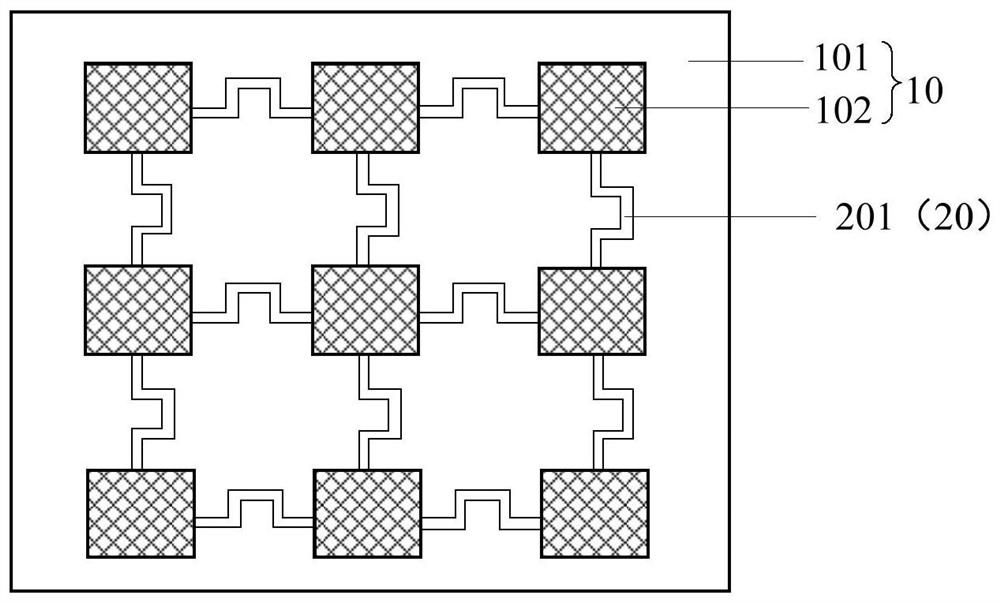
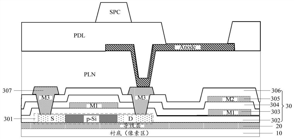
[0027] The present application provides an array substrate. The array substrate includes a substrate with a stretchable flexible area and a non-stretchable pixel area. In the pixel area, the shear force between the flexible substrate and the pixel island can be eliminated, reducing the risk of peeling off of the pixel island and also reducing the risk of wire layer breakage.
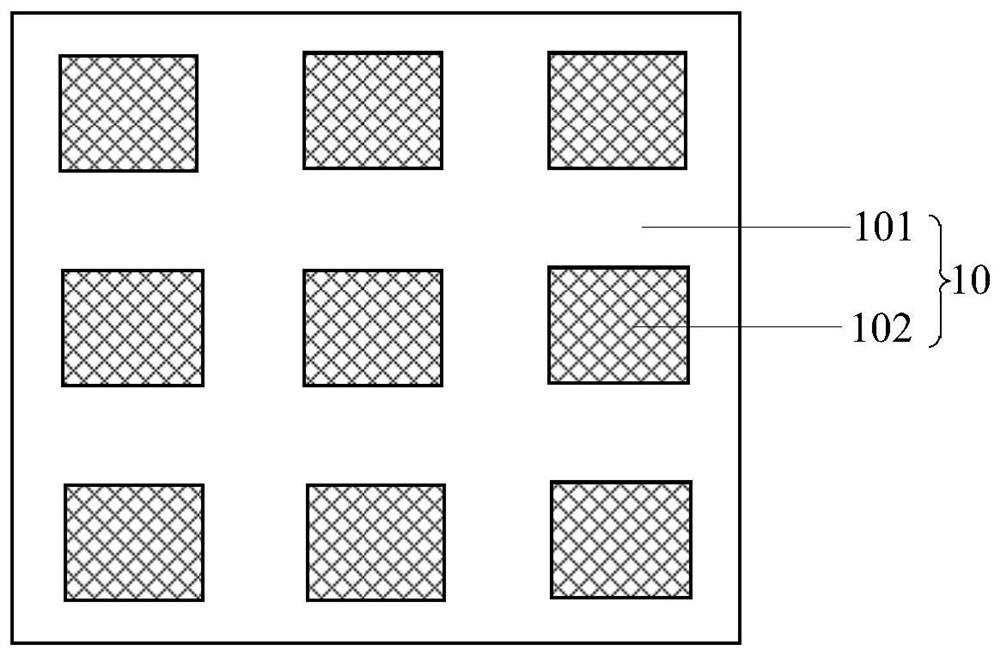
[0028] see figure 1 , figure 1 is a schematic top view structure diagram of the substrate in the embodiment of the present application. In this embodiment, a substrate is provided, and the substrate 10 includes a stretchable flexible region 101 and a non-stretchable pixel region 102 . The substrate 10 is a flexible substrate with stretchability. When the substr...
PUM
 Abstract
Description
Claims
Application Information