Chip IP integration method and device, electronic equipment and storage medium

An integrated method and chip design technology, applied in CAD circuit design, electrical digital data processing, computer-aided design, etc., can solve problems such as human error and time-consuming, and achieve the effect of improving work efficiency and reducing the probability of human error

Active Publication Date: 2020-10-30
SHANDONG YUNHAI GUOCHUANG CLOUD COMPUTING EQUIP IND INNOVATION CENT CO LTD
View PDF11 Cites 11 Cited by
  • Summary
  • Abstract
  • Description
  • Claims
  • Application Information

AI Technical Summary

Problems solved by technology

Complex IP has many external interfaces, manual integration not only takes a long time, but also easily causes human errors

Method used


Image

  • Chip IP integration method and device, electronic equipment and storage medium
  • Chip IP integration method and device, electronic equipment and storage medium
  • Chip IP integration method and device, electronic equipment and storage medium

Examples


Embodiment Construction

[0047] The following will clearly and completely describe the technical solutions in the embodiments of the application with reference to the drawings in the embodiments of the application. Apparently, the described embodiments are only some of the embodiments of the application, not all of them. Based on the embodiments in this application, all other embodiments obtained by persons of ordinary skill in the art without making creative efforts belong to the scope of protection of this application.

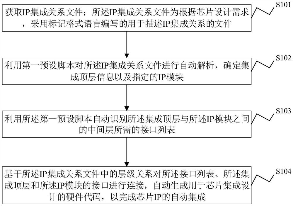
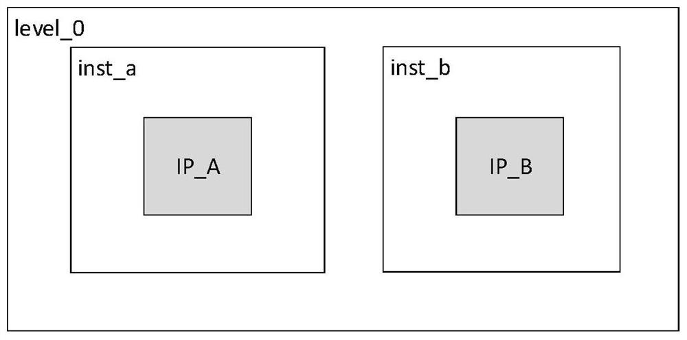
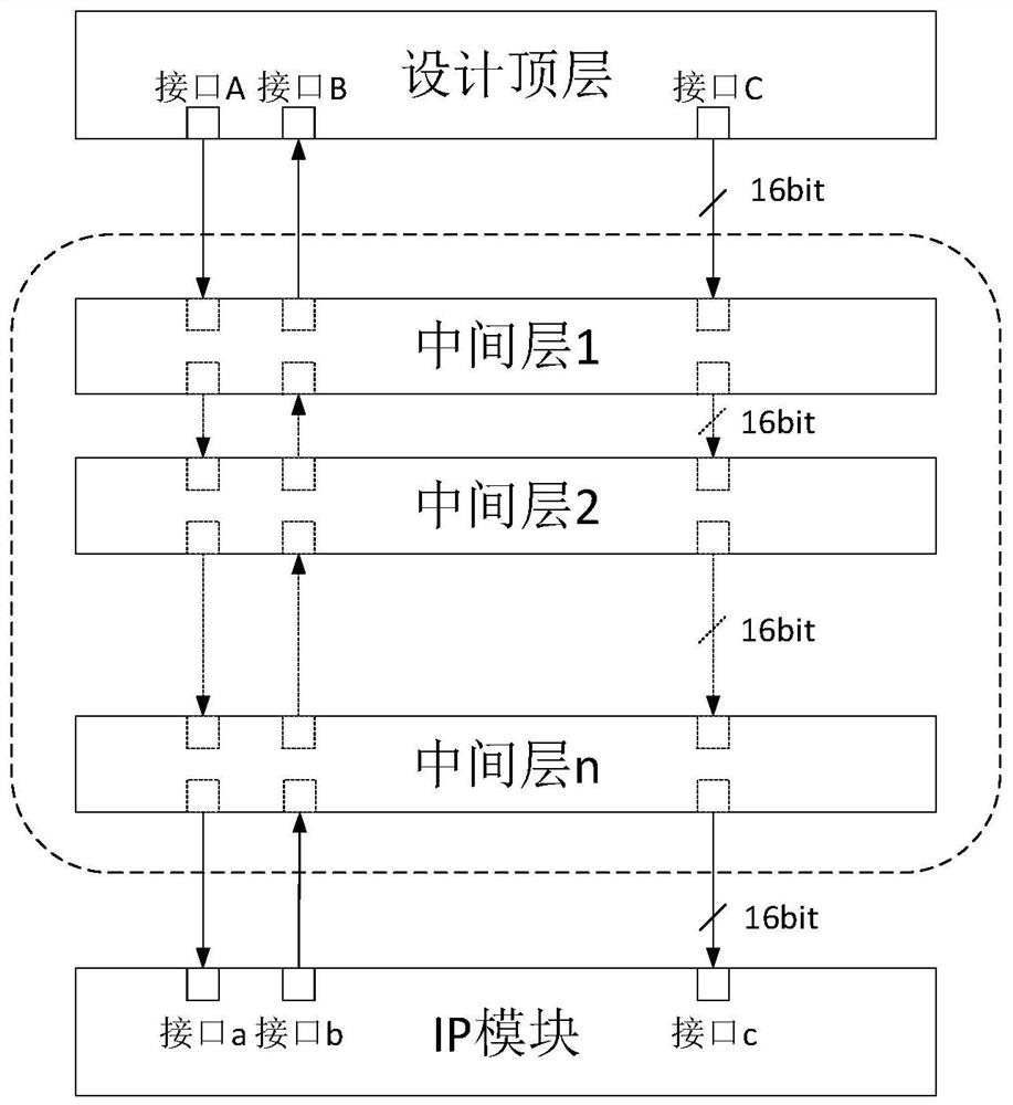
[0048] In related technologies, chip IP is usually developed by VHDL or Verilog language. Chip designers need to study IP code carefully and manually integrate IP with existing chip design code. Complex IP has many external interfaces, and manual integration not only takes a long time, but also easily causes human errors.

[0049] Therefore, the embodiment of the present application discloses a chip IP integration method, which significantly reduces the probability of human error wh...


PUM


Abstract

The invention discloses a chip IP integration method and device, electronic equipment and a storage medium. The method comprises the steps of obtaining an IP integration relationship file which is written by adopting a markup format language and is used for describing an IP integration relationship according to a chip design demand; automatically analyzing the IP integration relation file by utilizing a first preset script, determining integration top layer information and a specified IP module, and automatically identifying an interface list required by a middle layer between an integration top layer and the IP module; and connecting the interface list, the integration top layer and the interface of the IP module based on the hierarchical relationship in the IP integration relationship file, and automatically generating hardware codes to complete automatic integration of chip IPs. According to the invention, the IP source code and the integration relationship of the chip can be automatically analyzed by utilizing the pre-written script according to the obtained integration relationship file, the required hardware code and the corresponding review report are generated, manual writing is not needed, and the human error probability is reduced while the working efficiency is improved.

Description

technical field [0001] The present application relates to the technical field of chip development, and more specifically, to a chip IP integration method and device, an electronic device, and a computer-readable storage medium. Background technique [0002] IP refers to a hardware description language program with specific circuit functions. This program has nothing to do with the integrated circuit process and can be transplanted to different semiconductor processes to produce integrated circuit chips. There are usually multiple IPs inside a chip, and IP integration refers to connecting IPs into the chip design. IP is commonly used in some digital circuits, but more complex functional modules, such as modems, SDRAM controllers, PCI interfaces, etc., can be designed as modules with modifiable parameters. Chip designers need to choose appropriate IP and integrate them together Build the chip. Selecting IP can avoid repeated development and accelerate product design. [000...

Claims


Application Information

Patent Timeline
Patent Type & Authority Applications(China)
IPC IPC(8): G06F30/32G06F115/08
CPCG06F30/32G06F2115/08
Inventor 沈欣舞王金富李磊樊光锋
Owner SHANDONG YUNHAI GUOCHUANG CLOUD COMPUTING EQUIP IND INNOVATION CENT CO LTD
Why Eureka
Try Eureka