Packaging detection equipment suitable for multi-specification semiconductors

A testing equipment, semiconductor technology, applied in the direction of single semiconductor device testing, semiconductor/solid-state device manufacturing, the use of mechanical devices, etc., can solve problems such as trouble

Inactive Publication Date: 2020-11-13
重庆信易源智能科技有限公司
View PDF0 Cites 0 Cited by
  • Summary
  • Abstract
  • Description
  • Claims
  • Application Information

AI Technical Summary

Problems solved by technology

[0004] The object of the present invention is to provide a package testing equipment suitable for multi-standard semiconductors, so as to solve the problem that many semiconductor package testing equipment in the background art can only test semiconductors of the same specification. The detection needs to be replaced by equipment, which brings a lot of trouble

Method used


Image

  • Packaging detection equipment suitable for multi-specification semiconductors
  • Packaging detection equipment suitable for multi-specification semiconductors
  • Packaging detection equipment suitable for multi-specification semiconductors

Examples


Embodiment Construction

[0026] The technical solutions in the embodiments of the present invention will be clearly and completely described below in conjunction with the accompanying drawings in the embodiments of the present invention. Obviously, the described embodiments are only some of the embodiments of the present invention, not all of them. Based on The embodiments of the present invention and all other embodiments obtained by persons of ordinary skill in the art without making creative efforts belong to the protection scope of the present invention.

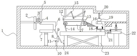
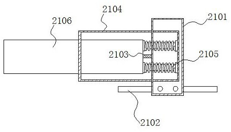
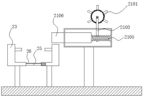
[0027] see Figure 1-5, the present invention provides a technical solution: a packaging and testing equipment suitable for multi-standard semiconductors, including a bracket 1, a first support plate 12 and a pushing device 21, a first tooth column 2 is installed on the left inner surface of the bracket 1, And the side of the first tooth column 2 is equipped with a transmission gear 3, the surface of the transmission gear 3 is equipped with a ro...


PUM


Abstract

The invention discloses packaging detection equipment suitable for multiple specifications of semiconductors. The equipment comprises a bracket, a first supporting plate and a pushing device. A firsttooth column is mounted on the inner surface of the left side of the bracket; a rocker is mounted on the surface of a transmission gear; a second toothed column is mounted on the side surface of the transmission gear; a detection table is mounted at the bottom of a touch rod in a deviating manner; a first rotating rod is mounted at the top of a sliding rod; a fixed rod is mounted at the bottom ofthe sliding rod; a first transmission rod is mounted on the surface of the conveying belt; a first push rod is mounted at the top of a bearing plate in a deviating manner; a connecting rod is mountedon the inner side of the material frame; a sponge pad is installed on the side face of the material frame, through the arrangement of the bearing plate and a first spring, when packaged products are transported to the bearing plate, the packaged products can stay in place due to the action of the first spring, then the packaged products are pushed to a material frame under the action of first pushrod, and the orderly transportation of the materials can be achieved.

Description

technical field [0001] The invention relates to the technical field of semiconductor package inspection, in particular to a package inspection device suitable for multi-standard semiconductors. Background technique [0002] Semiconductor refers to a material whose conductivity is between that of a conductor and an insulator at room temperature. It has applications in integrated circuits, consumer electronics, communication systems, photovoltaic power generation, lighting, high-power power conversion, etc., whether in terms of technology or economic development. From the point of view, the importance of semiconductors is very huge. The core units of most electronic products, such as computers, mobile phones or digital recorders, are closely related to semiconductors. Because semiconductors are so important, so Semiconductors are packaged and inspected before they leave the factory. [0003] The existing semiconductor packaging testing equipment can accurately detect the defe...

Claims


Application Information

Patent Timeline
Patent Type & Authority Applications(China)
IPC IPC(8): G01R31/26G01R31/01G01R1/04G01B5/06G01B5/02H01L21/67
CPCG01B5/02G01B5/06G01R1/0408G01R31/013G01R31/2601H01L21/67242
Inventor 胡蓓张万娟
Owner 重庆信易源智能科技有限公司
Why Eureka
Try Eureka