
A Reconfigurable Dual Beam Periodic Leaky-Wave Antenna
A leaky wave antenna and periodic technology, applied in the field of communication antennas, to achieve the effect of flexible and variable beam coverage
- Summary
- Abstract
- Description
- Claims
- Application Information
AI Technical Summary
Problems solved by technology
Method used
Image


Examples
Embodiment 1
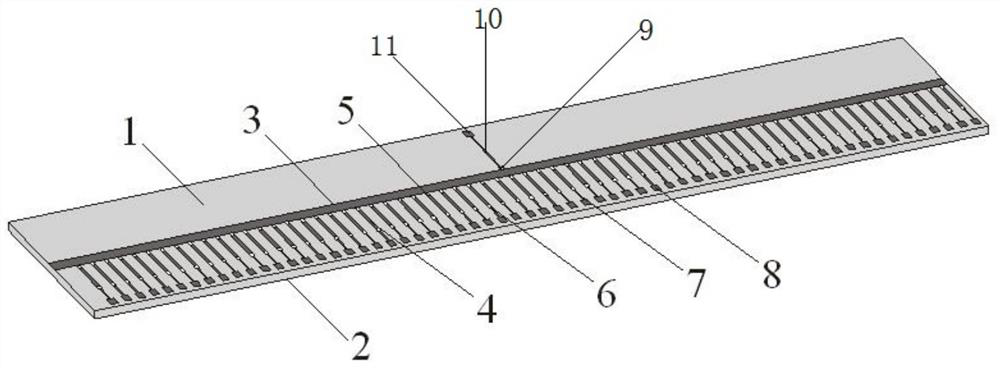
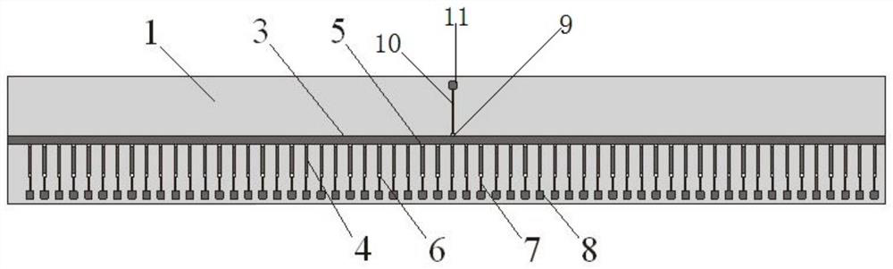
[0047] like figure 1 , figure 2 , image 3 As shown, a reconfigurable dual-beam periodic microstrip leaky wave antenna includes a metal floor 2, a microstrip line 3, a stub 4, a dielectric plate 1, a PIN diode 5, a first inductor 6, a first direct Current bias line 7, first DC pad 8, second inductor 9, second DC bias line 10, second DC pad 11;
[0048]The microstrip line 3 and the stub 4 are located on the upper surface of the dielectric board 1, and the metal floor 2 is located on the lower surface of the dielectric board 1;
[0049] One end of the PIN diode 5 is connected to one side of the microstrip line 3 , and the other end of the PIN diode 5 is connected to one end of the stub 4 ; the other end of the stub 4 is connected to one end of the first inductor 6 . connected; the other end of the first inductor 6 is connected to one end of the first DC bias line 7; the other end of the first DC bias line 7 is connected to the first DC pad 8;
[0050] The PIN diode 5, the s...
PUM
| Property | Measurement | Unit |
|---|---|---|
| length | aaaaa | aaaaa |
| width | aaaaa | aaaaa |
| width | aaaaa | aaaaa |
Abstract
Description
Claims
Application Information