OLED display panle and a package method

a technology of organic light-emitting diodes and display panels, which is applied in the field of display, can solve the problems of apparent decay of brightness and and achieve the effects of improving efficiency, improving packaging effect, and increasing the life of oled devices

Active Publication Date: 2018-12-11
TCL CHINA STAR OPTOELECTRONICS TECH CO LTD
View PDF15 Cites 1 Cited by
  • Summary
  • Abstract
  • Description
  • Claims
  • Application Information

AI Technical Summary

Benefits of technology

[0005]The present invention is to provide an Organic Light-Emitting Diode (OLED) display panel and a package method thereof, for blocking moisture and oxygen from penetrate into the hermetic space and influencing the performance of the organic thin film. The package effect is improved and the life of the OLED device is increased.
[0020]The benefit of the present invention is that the supporter and the hydrophobic wall are printed simultaneously on the outer position of the OLED device by screen printing, wherein the hydrophobic wall is set on outer position of the supporter 13 to block moisture and oxygen from contacting the OLED device. The organic thin film of the OLED device is particularly influenced and the package effect is improved and the life of the OLED device is increased. Furthermore, the supporter and the hydrophobic wall are formed simultaneously so this method is easy and efficiency is improved.

Problems solved by technology

Brightness and life of the OLED device apparently decays.

Method used


Image

  • OLED display panle and a package method
  • OLED display panle and a package method

Examples


Embodiment Construction

[0026]To better and concisely explain the disclosure, the same name or the same reference number given or appeared in different paragraphs or figures along the specification should has the same or equivalent meanings while it is once defined anywhere of the disclosure.

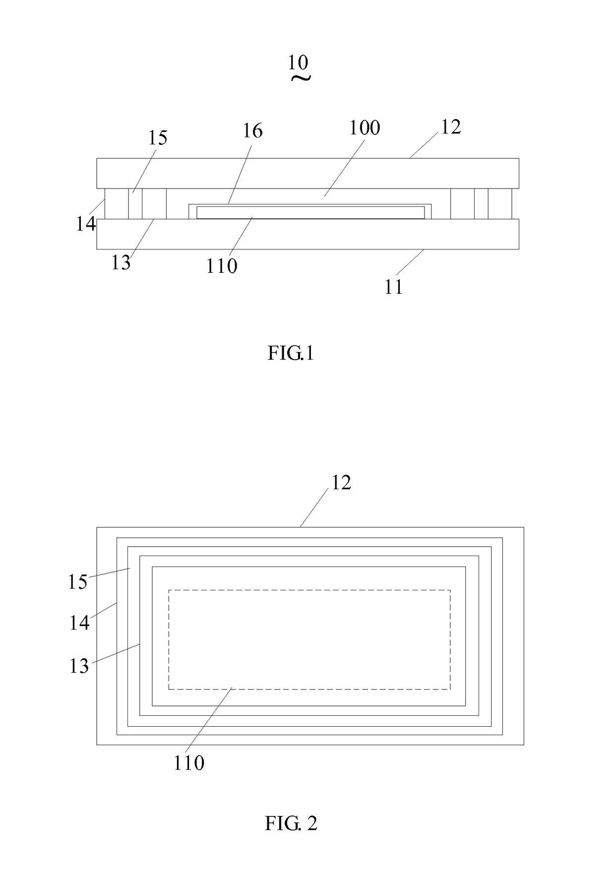
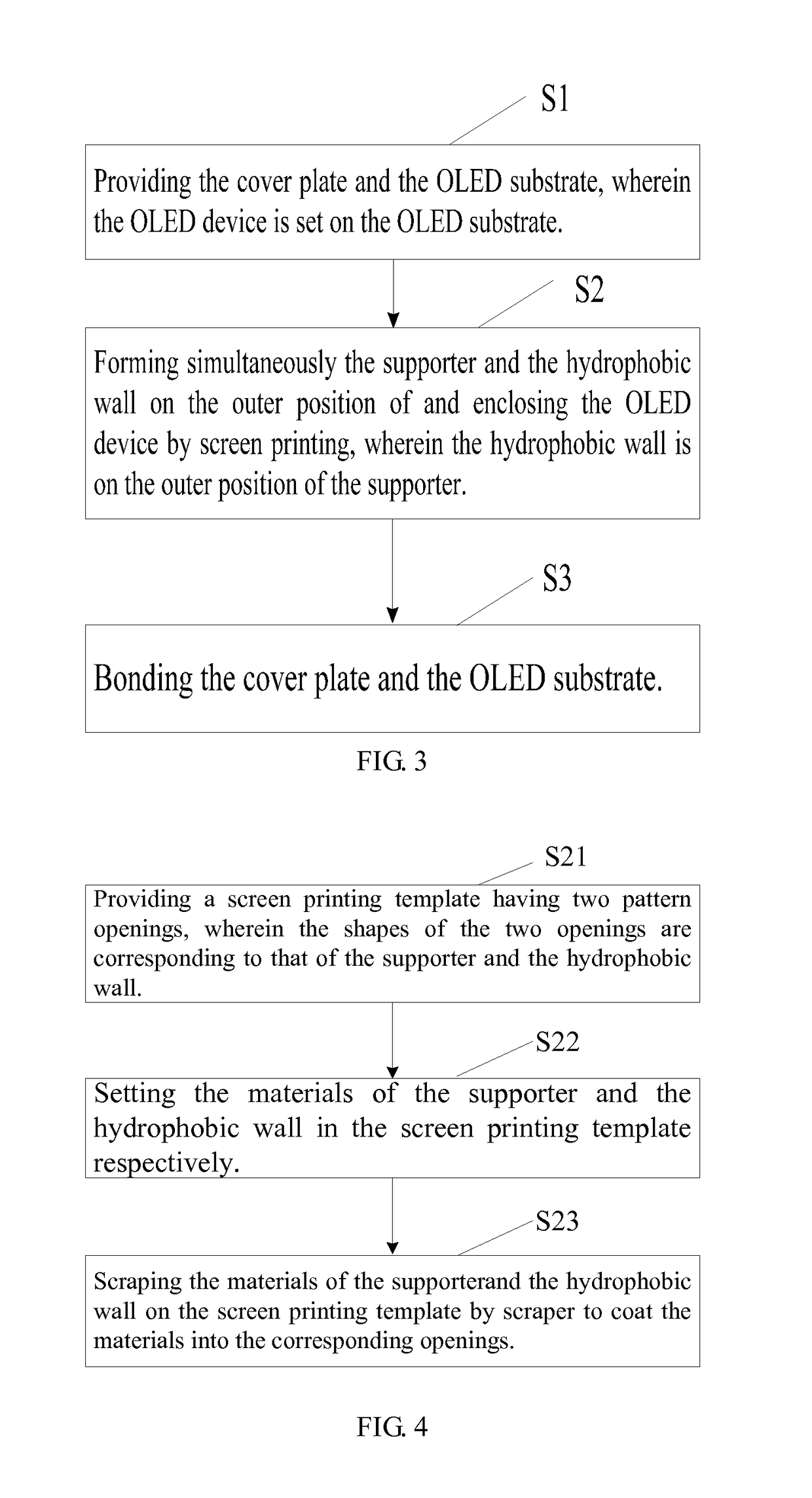
[0027]FIG. 1 is a schematic diagram of a structure of an OLED display panel in accordance with an embodiment of the present invention. The OLED display panel 10 includes an OLED substrate 11, a cover plate 12, a supporter 13, and a hydrophobic wall 14, wherein an OLED device 110 is formed on the OLED substrate 11.

[0028]Referring to FIG. 2 which is a schematic diagram of a structure of the cover plate 12, the supporter 13 is printed on the cover plate 12 by screen printing and located on outer position of the OLED device 110. The supporter 13 encloses the OLED device 110 when the OLED substrate 11 and the cover plate 12 are bonded. The hydrophobic wall 14 is printed on the cover plate 12 by screen printing and located o...


PUM


Abstract

The present invention is to provide an Organic Light-Emitting Diode (OLED) display panel and a package method thereof. The method includes forming simultaneously a supporter and a hydrophobic wall on an outer position of and enclosing the OLED device by screen printing, wherein the hydrophobic wall is on an outer position of the supporter; and bonding the cover plate and the OLED substrate. The present invention can effectively protect the OLED device from outer moisture and oxygen to improve package effect and increase life of the OLED device. The supporter and the hydrophobic wall are formed simultaneously by screen printing so the method is simple and the manufacturing efficiency is improved.

Description

BACKGROUND[0001]Technical Field[0002]The present invention relates to display field, and more particularly, to an Organic Light-Emitting Diode (OLED) display panel and a package method thereof.[0003]Description of Related Art[0004]An Organic Light-Emitting Diode (OLED) display is a display of new generation. An organic thin film is formed on an OLED substrate and between an anode and a cathode. Forward voltage is applied to the anode and the cathode and the organic thin film emits light. The organic thin film is sensitive to the moisture and oxygen and thus degenerates. Brightness and life of the OLED device apparently decays. Therefore, the OLED device needs package process. The conventional package method includes coating UV glue on the periphery of the cover plate, bonding the OLED substrate and the cover plate, forming a hermetic space among two glass substrates and support elements formed by the UV glue, and setting the organic thin film in the hermetic space. Because ability o...

Claims


Application Information

Patent Timeline
Patent Type & Authority Patents(United States)
IPC IPC(8): H01L21/00H01L51/52H01L27/32H01L51/56
CPCH01L27/32H01L51/56H01L51/524H01L2251/301H10K59/00H10K50/8426H10K71/00H10K50/841H10K2102/00
Inventor YU, WEI
Owner TCL CHINA STAR OPTOELECTRONICS TECH CO LTD
Why Eureka
Try Eureka