Unlock instant, AI-driven research and patent intelligence for your innovation.
Semiconductor device
Inactive Publication Date: 2002-09-12
SEMICON ENERGY LAB CO LTD
View PDF48 Cites 89 Cited by
Summary
Abstract
Description
Claims
Application Information
AI Technical Summary
This helps you quickly interpret patents by identifying the three key elements:
Problems solved by technology
Method used
Benefits of technology
Benefits of technology
[0317] According to the present invention in the application, in the semiconductor device in which the semiconductor display device capable of displaying a still image (or moving image with a short time) is incorporated, the memory portion is mounted on the substrate on which the pixel portion is formed. As result, there are provided the semiconductor display device capable of suppressing consumption power to low in the case where the still image is displayed and the semiconductor device in which the semiconductor display device is incorporated.[0318] Also, according to the present invention in the application, the memory portion and the memory control circuit may be provided on the substrate on which the pixel portion is formed. When such a structure is used, the still image (or moving image with a short time) can be displayed by inputting only simple control signals from the outside of the substrate on which the pixel portion is formed. Thus, the semiconductor display device having low consumption power and the semiconductor device in which the semiconductor display device is incorporated are realized.
Problems solved by technology
On the other hand, in the active matrix display device using the amorphous silicon films and the passive matrix display device, it is difficult to integrally form the driver circuits on a substrate on which the pixel portion is formed.
Method used
Image
Click on the blue label to locate the original text in one second.
Reading with bidirectional positioning of images and text.
Examples
embodiment 1
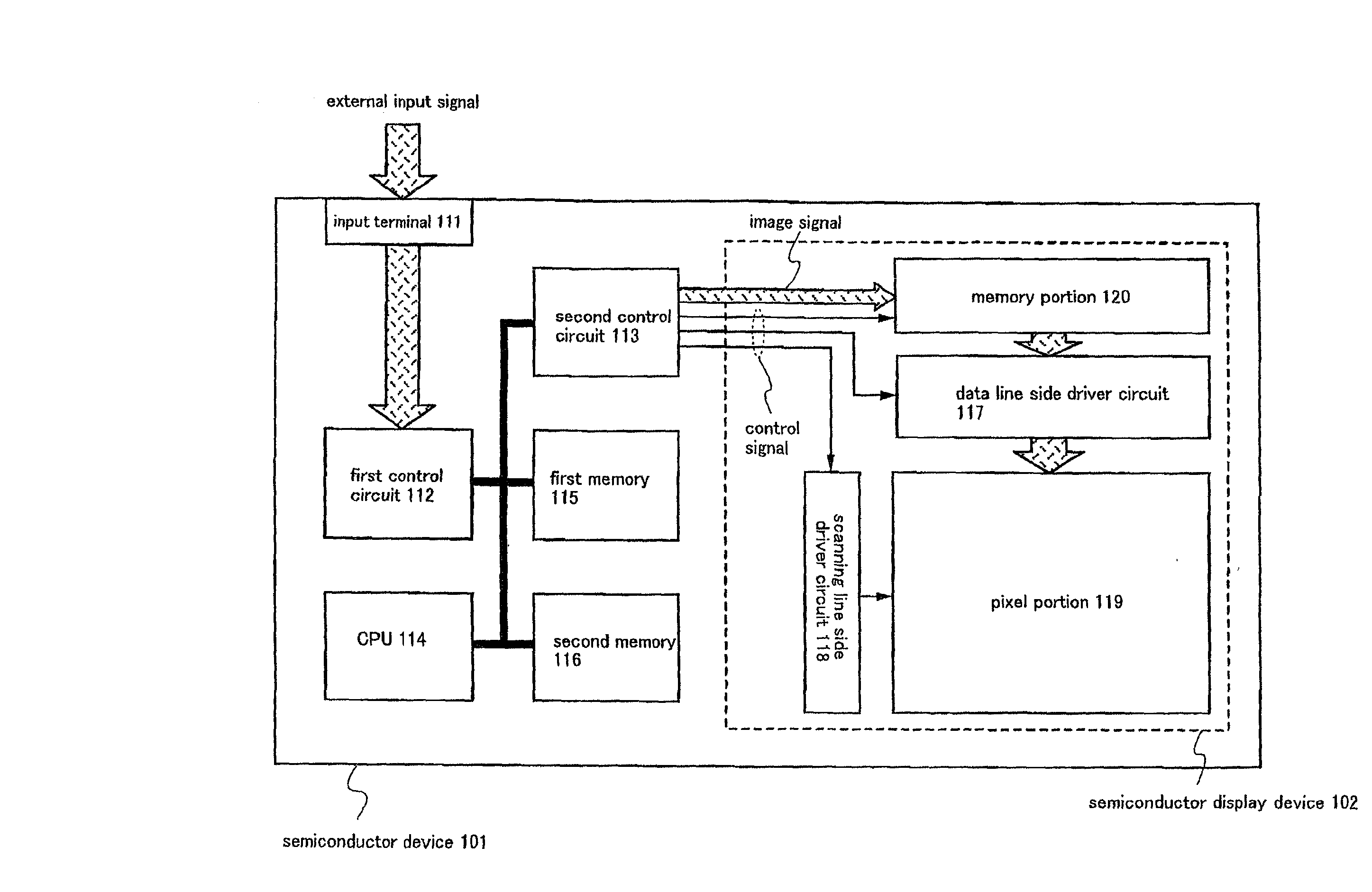
[0127] In the present invention in the application, it is preferable that a memory control circuit is mounted on a substrate on which the pixel portion is formed.
[0128] FIGS. 5 and 6 are block diagrams of a semiconductor device in which a semiconductor display device having a memory control circuit is incorporated. Portions except for the semiconductor display devices comprise input terminals 511 and 611, first control circuits 512 and 612, second control circuits 513 and 613, CPUs 514 and 614, first memories 515 and 615, second memories 516 and 616, respectively, and similar to the case of the semiconductor device (see FIG. 1) described in the embodiment mode. In a semiconductor display device 502 shown in FIG. 5, a memory control circuit 517 is integrally formed with a memory portion 521, a data line side driver circuit 518, a scanning line side driver circuit 519, and a pixel portion 520 on the same substrate. Further, in a semiconductor display device 602 shown in FIG. 6, stick ...
embodiment 2
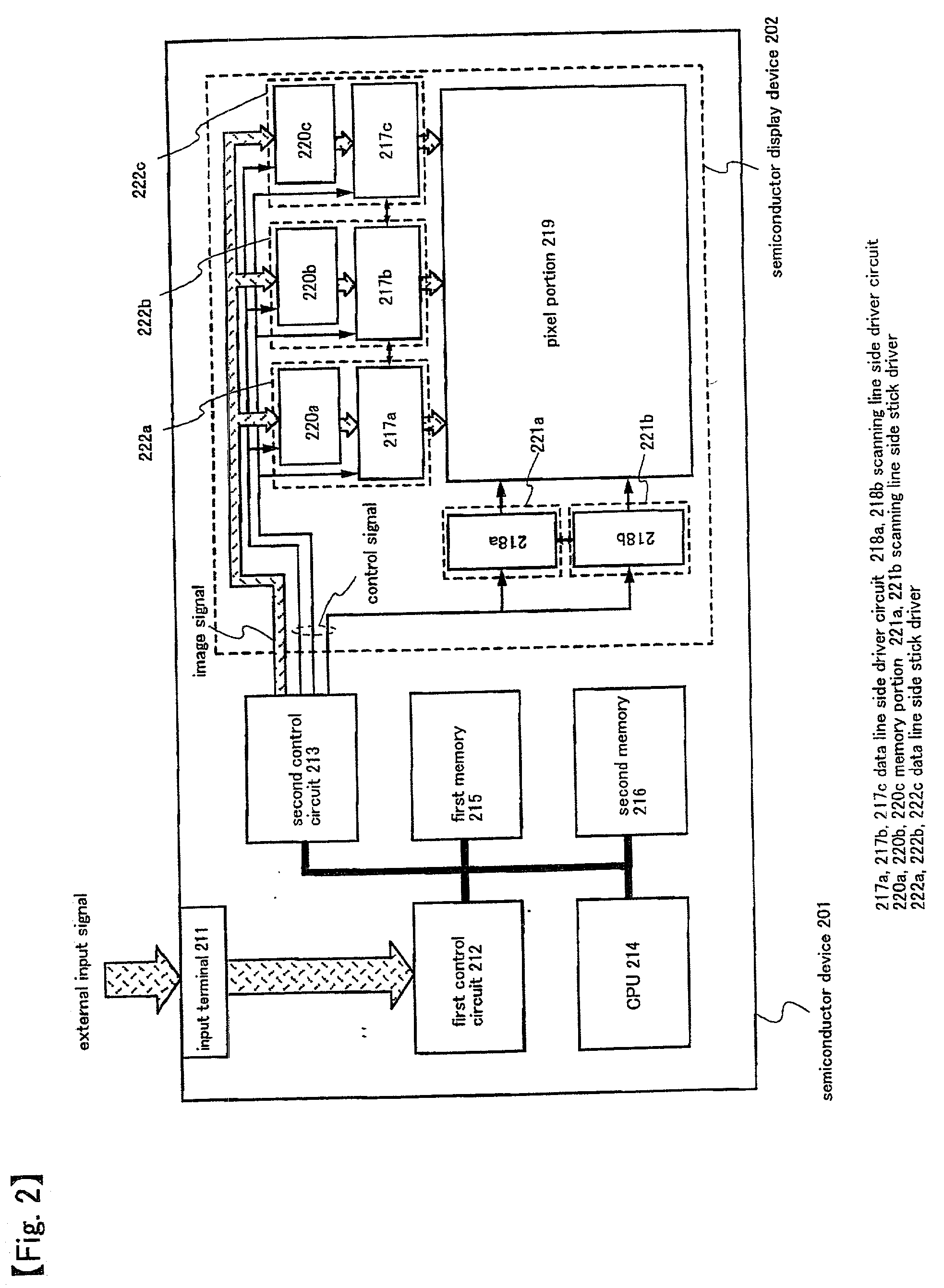
[0132] The semiconductor devices (FIGS. 1 and 2) described in the embodiment mode can be also considered as two independent semiconductor devices. In this embodiment, of the two independent semiconductor devices, a semiconductor device including a semiconductor display device will be described. The description is made using FIGS. 7 and 8.
[0133] The semiconductor device 701 shown in FIG. 7 comprises an input terminal 711, a control circuit 712, and a semiconductor display device 702. In the semiconductor display device 702, a memory portion 714 is integrally formed with a pixel portion 717, a data line side driver circuit 715, and a scanning line side driver circuit 716 on the same substrate. On the other hand, the semiconductor device 801 shown in FIG. 8 comprises an input terminal 803, a control circuit 804, and a semiconductor display device 802. In the semiconductor display device 802, memory portions 820a, 820b, and 820c and data line side driver circuits 817a, 817b, and 817c ar...
embodiment 3
[0137] In this embodiment, an example that the present invention in the application is applied to an active matrixliquid crystal display device will be described. The description is made using FIG. 9.
[0138] FIG. 9(A) is a block diagram of an active matrixliquid crystal display device. The active matrix liquid crystal display device shown in FIG. 9(A) has a pixel portion 901 in which pixels 904 are arranged in matrix, a data line side driver circuit 902, a scanning line side driver circuit 903, and a memory portion 905. Data lines 906 are connected with the data line side driver circuit 902. Scanning lines 907 are connected with the scanning line side driver circuit 903. A common potential is provided for a capacitor line 908.
[0139] Note that the pixel portion 901, the data line side driver circuit 902, the scanning line side driver circuit 903, and the memory portion 905 may be formed on the same substrate. Further, the data line side driver circuit 902, the memory portion 905, an...
PUM
Abstract
A semiconductor device capable of displaying a still image with low consumption power is provided. In the semiconductor device incorporated with a semiconductordisplay device capable of displaying the still image, a memory portion is mounted on a substrate on which a pixel portion is formed. As a mounting method, the memory portion is formed on the substrate on which the pixel portion is formed or a stick driver including the memory portion is used. When the still image is displayed using image data stored in such a memory portion, the still image can be displayed by inputting only simple control signals from the outside of the semiconductor device. Thus, there are provided the semiconductor display device capable of displaying the still image with low consumption power and the semiconductor device incorporated with the semiconductor display device.
Description
TECHNICAL FIELD TO WHICH THE INVENTION BELONGS[0001] The present invention in the application relates to a semiconductor device having a pixel portion, a driver circuits for the pixel portion, and a memory portion.[0002] In particular, the present invention relates to a semiconductor display device in which a pixel portion, driver circuits for the pixel portion, and a memory portion are integrally formed on the same substrate, a semiconductor display device in which a second substrate is mounted on a first substrate for forming a pixel portion, driver circuits for the pixel portion and a memory portion are integrally formed in the second substrate, and an electronic equipment in which such a semiconductor display device is incorporated.[0003] Note that a semiconductor device in this specification indicates a device in general, which functions by utilizing a semiconductor characteristic, and includes for example, a semiconductor display device which represents a liquid crystal displa...
Claims
Application Information
Patent Timeline
Application Date:The date an application was filed.
Publication Date:The date a patent or application was officially published.
First Publication Date:The earliest publication date of a patent with the same application number.
Issue Date:Publication date of the patent grant document.
PCT Entry Date:The Entry date of PCT National Phase.
Estimated Expiry Date:The statutory expiry date of a patent right according to the Patent Law, and it is the longest term of protection that the patent right can achieve without the termination of the patent right due to other reasons(Term extension factor has been taken into account ).
Invalid Date:Actual expiry date is based on effective date or publication date of legal transaction data of invalid patent.

