Assembling structure of electronic apparatus and assembling method thereof

a technology of electronic equipment and assembling structure, which is applied in the direction of electrical apparatus casing/cabinet/drawer, transportation and packaging, coupling device connection, etc., can solve the problems of inability to miniaturize, print circuit board, and high probability of bad welding, so as to facilitate the use of inner space and miniaturize the electronic apparatus

Inactive Publication Date: 2005-12-15
DELTA ELECTRONICS (THAILAND) PUBLIC CO LTD +1
View PDF13 Cites 3 Cited by
  • Summary
  • Abstract
  • Description
  • Claims
  • Application Information

AI Technical Summary

Benefits of technology

[0007] An object of the present invention is to provide an assembling structure of an electronic apparatus and the assembling method thereof to facilitate the uses of the inner space of the electronic apparatus and the wiring area of the printed circuit board, so as to miniaturize the electronic apparatus.

Problems solved by technology

Moreover, the aforesaid welding process is not easy to perform, so a bad welding is likely to happen.
In addition, for the reason that the electronic elements of the printed circuit board 13 are connected and fixed by the surface mount technology (SMT), which needs a certain welding area provided on the printed circuit board 13, the printed circuit board 13 cannot be miniaturized, and the limited wiring space will become denser and more complex, which indirectly affects the electromagnetic compatibility (EMC) of the electronic apparatus.

Method used


Image

  • Assembling structure of electronic apparatus and assembling method thereof
  • Assembling structure of electronic apparatus and assembling method thereof
  • Assembling structure of electronic apparatus and assembling method thereof

Examples


Embodiment Construction

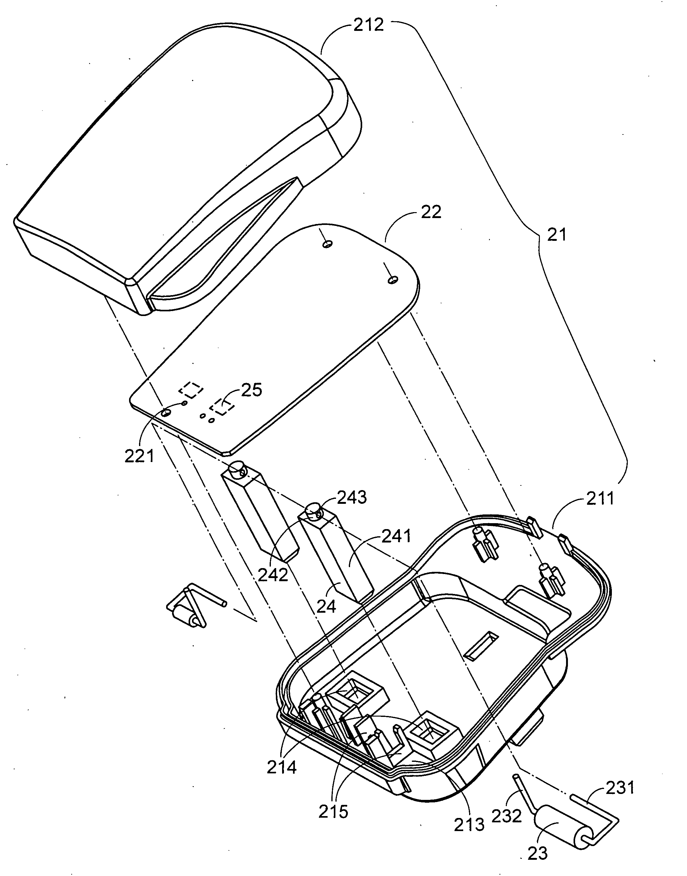
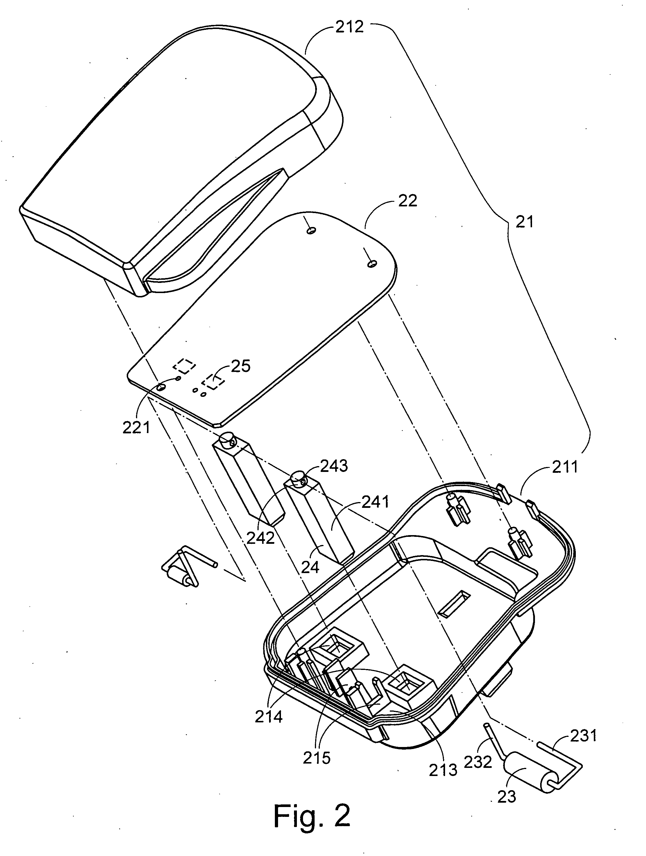
[0026] Please refer to FIG. 2, which is a schematic view showing an assembling structure of an electronic apparatus according to the preferred embodiment of the present invention. As shown in FIG. 2, the assembling structure of the electronic apparatus in the present invention mainly comprises a casing 21, a printed circuit board 22, one or more electronic elements 23, and a plurality of conductive terminals 24. The casing 21 comprises a first isolation casing 211 and a second isolation casing 212. The printed circuit board 22 is disposed in a receiving space 213 of the casing 21 and provides different power conversion functions via different circuit layouts and different dispositions of the electronic elements. The plurality of conductive terminals 24 are disposed on the first isolation casing 211 and electrically connected with the printed circuit board 22 for conducting the external power into the printed circuit board so as to enable the electronic apparatus to perform its funct...


PUM

PropertyMeasurementUnit
structureaaaaaaaaaa
conductiveaaaaaaaaaa
assembling structureaaaaaaaaaa

Abstract

An assembling structure of an electronic apparatus and the assembling method thereof are disclosed. The assembling structure of an electronic apparatus comprises a casing having a receiving space, a plurality of conductive terminals, a printed circuit board and at least an electronic element. The plurality of conductive terminals are disposed on the casing, and each conductive terminal has a first part extending to the outer side of the casing and a second part extending to the inner side of the casing, wherein the second part has a through hole. The printed circuit board is disposed in the receiving space and has at least a conductive element and a plurality of conductive pads, wherein the plurality of conductive pads contact the second parts of the plurality of conductive terminals. The electronic element has a first linking bar and a second linking bar, wherein the first linking bar passes through the through hole, and the second linking bar connects with the conductive element of the printed circuit board.

Description

FIELD OF THE INVENTION [0001] The present invention relates to an assembling structure of an electronic apparatus and the assembling method thereof, and more particularly to an assembling structure of an adaptor and the assembling method thereof. BACKGROUND OF THE INVENTION [0002] With the progress of science and technology day by day, various electronic apparatuses such as adaptors have been broadly used in the daily life. Because the design of the electronic apparatus heads toward the development trend of high power and miniaturization, the disposition and assembling method of the electronic elements in the electronic apparatus become an important consideration to solve the miniaturization and electromagnetic compatibility (EMC) problems. [0003] Please refer to FIG. 1, which is a schematic view showing the assembling structure of a conventional electronic apparatus. As shown in FIG. 1, the conventional electronic apparatus comprises a casing 11, a plurality of conductive terminals...

Claims


Application Information

Patent Timeline
Patent Type & Authority Applications(United States)
IPC IPC(8): H01R13/66H01R31/06H05K5/00
CPCH01R13/6658H01R24/28Y10T29/4913H01R2103/00Y10T29/49126H01R31/065
Inventor LIM, CHOO SOOCHAISRI, PHUMCHAI
Owner DELTA ELECTRONICS (THAILAND) PUBLIC CO LTD
Why Eureka
Try Eureka