Display device with metal-organic mixed layer anodes

Active Publication Date: 2006-11-23
LG DISPLAY CO LTD
View PDF99 Cites 37 Cited by
  • Summary
  • Abstract
  • Description
  • Claims
  • Application Information

AI Technical Summary

Problems solved by technology

When viewed under high ambient illumination, the reflective back electrode reflects a substantial amount of the ambient illumination to the observer, which results in higher ratios of reflected illumination as compared to the device's own emission resulting in “washout” of the displayed image.
The use of ITO has disadvantages, however, in that ITO cannot be readily fabricated by thermal vapor deposition techniqu

Method used


Image

  • Display device with metal-organic mixed layer anodes

Examples


examples 1-16

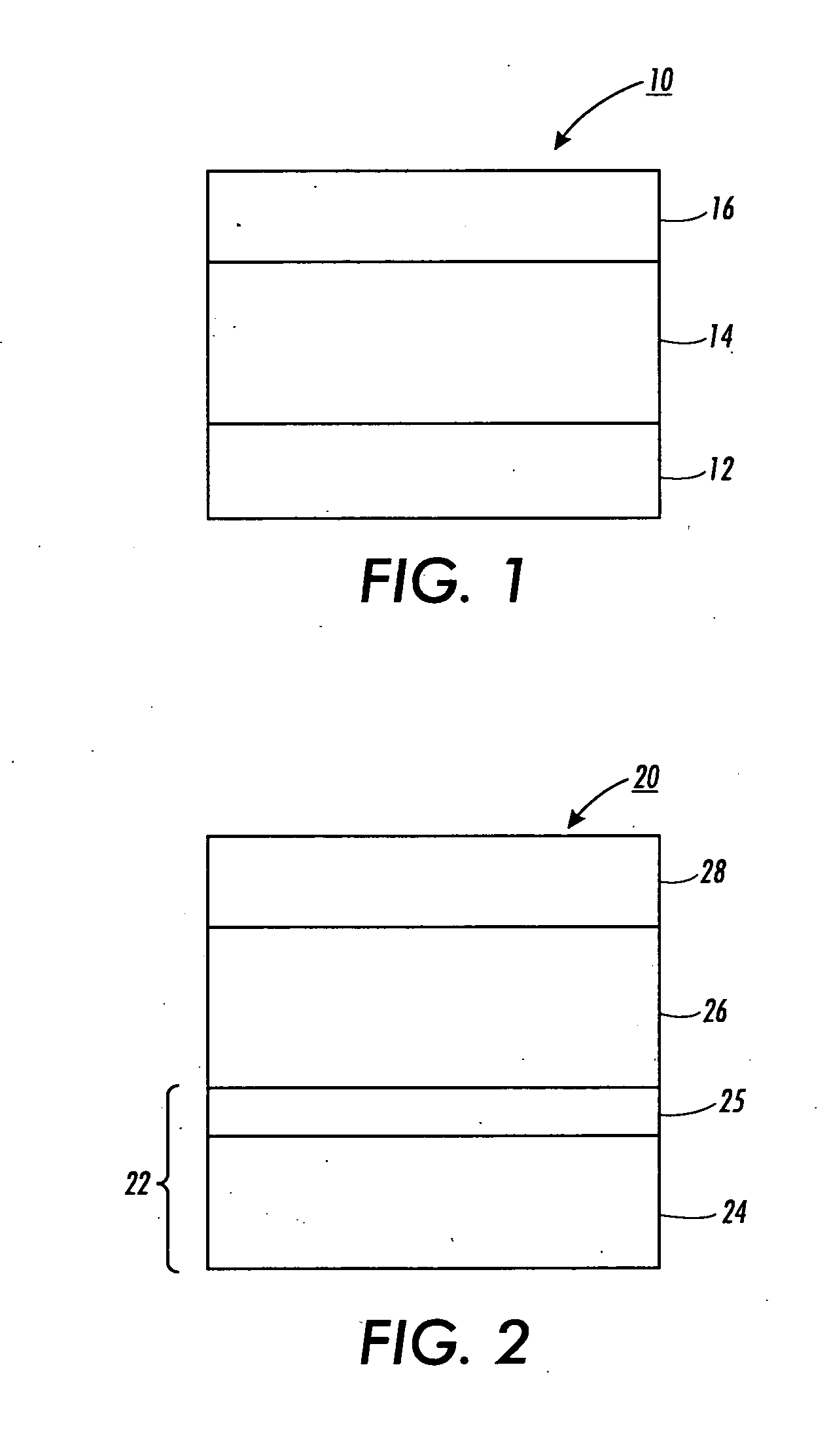
[0074] Examples 1-16 in Table 1 below summarize OLED devices that have been reduced to practice. All devices were fabricated using physical vapor deposition in vacuum (5×10⁻⁶ Torr). Table 1 indicates the anode configure used in the respective OLED devices. The luminescent region of the devices was composed of two layers: (i) a 600 angstrom NPB layer functioning as a hole transport zone, and (ii) a 750 angstrom AlQ3 layer serving the dual functions of light emission and electron transport. The cathode was formed with Mg:Ag. The NPB, AlQ3 and cathode layers were sequentially deposited following deposition of the anode layer. In samples 1-5, the anode had a configuration comprising a MOML and a buffer layer deposited over the MOML, wherein the buffer layer was a single layer entirely composed of an electron-accepting material. In examples 6-8, the anode comprised a MOML and a single layer buffer layer disposed over the MOML, the buffer layer configuration comprising an electron-accepti...

examples 17-21

[0076] Examples 17-21 were prepared in the same manner as described with reference to examples 1-16 and include the anode configuration set forth in Table 2. Examples 18-21 comprise anode configurations in accordance with the present disclosure and example 17 is a comparative example comprising a conventional ITO anode. The concentration of the components of the MOML are given in parenthesis next to the respective components and the number in parenthesis refer to the layer thickness in angstroms. As show in Table 2, different optical properties ranging from substantially transparent (as indicated by large SEIR values) to light-absorbing or dark (as indicated by small SEIR values) can be achieved by simply varying the thickness or composition of the MOML.

TABLE 2ExampleNo.Anode ConfigurationSEIR17ITO79.60%18AIQ3(90%) + Ag(10%)(150 Å) / F4-TCNQ(50 Å)72.50%19AIQ3(90%) + Ag(10%)(500 Å) / F4-TCNQ(50 Å)58.40%20AIQ3(80%) + Ag(20%)(1000 Å) / F4-TCNQ(50 Å)15.80%21AIQ3(80%) + Ag(20%)(2000 Å) / F4-TC...


PUM

PropertyMeasurementUnit
Fractionaaaaaaaaaa
Percent by volumeaaaaaaaaaa

Abstract

A display device comprises an anode, a cathode, and a luminescent region disposed between the anode and the cathode, wherein the anode comprises a metal-organic mixed layer operatively combined with an electron-accepting material. An anode may comprise a mixture of a metal-organic mixed layer and an electron-accepting material within a single layer of the anode. Alternatively, the anode may have a multilayer configuration comprising a metal-organic mixed layer and a buffer layer adjacent the metal-organic mixed layer, wherein the buffer layer comprises an electron-accepting material and optionally a hole transport material.

Description

INCORPORATION BY REFERENCE [0001] Co-pending Application No. ______ [A3623-US-NP] describes stacked OLEDs that may comprise as an intermediate electrode a metal-organic mixed layer in combination with an electron-accepting material. BACKGROUND [0002] The present disclosure relates, in various exemplary embodiments, to display devices comprising a metal-organic mixed layer as part of an anode configuration. In particular, the present disclosure relates to display devices comprising a metal-organic mixed layer as part of an anode and operatively combined with an electron-accepting material. While the anode configurations are described with particular reference to organic light emitting devices (OLEDs), it will be appreciated that the anodes are amendable to other similar applications and display devices. [0003] Organic light emitting devices (OLEDs) represent a promising technology for display applications. A typical organic light emitting device includes a first electrode; a luminesc...

Claims


Application Information

Patent Timeline
IPC IPC(8): H01L51/52H05B33/26
CPCH01L51/0053Y10S428/917H01L51/5206H01L51/0081H10K85/621H10K85/324H10K50/17H10K50/81H10K50/818H10K50/865H10K85/115H10K85/111H10K85/60H10K85/113H10K85/30H05B33/26C09K11/06
Inventor AZIZ, HANYSTEFANOVIC, NEMANJACOGGAN, JENNIFER A.PAINE, ANTHONY J.POPOVIC, ZORAN
Owner LG DISPLAY CO LTD
Why Eureka
Try Eureka