Semiconductor memory device

Active Publication Date: 2007-01-04
SK HYNIX INC
View PDF7 Cites 12 Cited by
  • Summary
  • Abstract
  • Description
  • Claims
  • Application Information

AI Technical Summary

Benefits of technology

[0051] In accordance with an aspect of the present invention, there is provided a semiconductor memory device, including: a memory cell block including a memory cell block including a N normal wordline and a M preliminary wordline; a refresh address counting block for outputting a refresh address, having a plurality of bits, corresponding to the N normal wordline and the M preliminary wordline; a refresh counting control block fo

Problems solved by technology

With technology advances, a memory capacity of the semiconductor memory device is increased and the semiconductor memory device is highly integrated to thereby increase a possibility of errors during a manufacturing process.
However, in above described operation, in case that the normal wordline and the preliminary wordline except a wordline coupled to cells having the defects are refreshed at the same time, the power consumption is twice as much as before.
Accordingly, a noise can occur because a voltage level, which is supplied to the wordline, drops instantaneously or the power level alters suddenly.
The noise is critical factor for amplifying data sensed from the unit cell; thus, it is impossible to exactly amplify the data inputted from the unit cell.
As the refresh operation is performed repeatedly with the noise, a risk of loss about the data stored in the unit cell dramatically increases.
Hence, despite no defects, a probability about a failure of the refresh operation increases.
In this case, it is impossible to guarantee whether the preliminary wordline is properly manufactured or not.

Method used


Image

  • Semiconductor memory device
  • Semiconductor memory device
  • Semiconductor memory device

Examples


Embodiment Construction

[0062] Hereinafter, a semiconductor memory device according to the present invention will be described in detail with reference to the accompanying drawings.

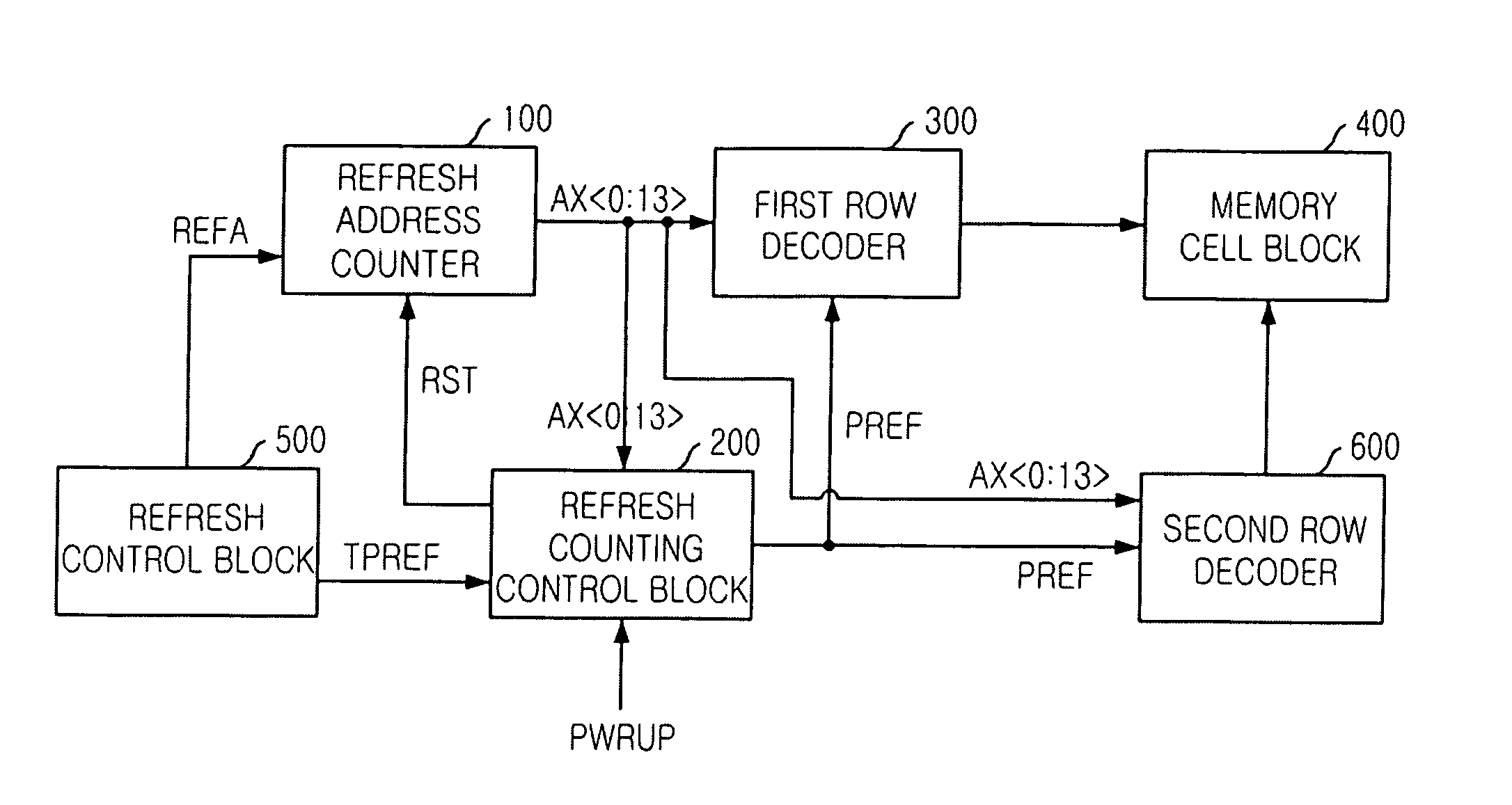
[0063]FIG. 5 is a block diagram showing a semiconductor memory device in accordance with an embodiment of the present invention.

[0064] As shown, the semiconductor memory device according to the embodiment of the present invention includes an normal wordline coupled to plural unit cells (e.g., 8K), a refresh address counter 100, a refresh counting control block 200, a row decoding block including a first row decoder 300 and a second row decoder 600, a memory cell block 400 and a refresh control block 500.

[0065] The memory cell block 400 includes a preliminary wordline (e.g., 128) for a replacement of the normal wordline coupled to a unit cell having defects. The refresh address counter 100 sequentially outputs a refresh address AX0:13>, corresponding to the 8K normal wordline and the 128 preliminary wordline. The refresh count...


PUM


Abstract

Disclosed herein is a semiconductor memory device for consuming a uniform amount of current. The semiconductor memory device includes a memory cell block including a N normal wordline and a M preliminary wordline; a refresh address counting block for outputting a refresh address, having a plurality of bits, corresponding to the N normal wordline and the M preliminary wordline; a refresh counting control block for resetting the refresh address counting block when the refresh address counts a predetermined count during a test mode; and a row decoding block for refreshing unit cells coupled to the N normal wordline and unit cells coupled to the M preliminary wordline of the memory cell block according to the refresh address and a redundancy control signal outputted from the refresh counting control block, wherein M, N are positive integers.

Description

FIELD OF THE INVENTION [0001] The present invention relates to a semiconductor memory device; and, more particularly, to a semiconductor memory device for performing an efficient refresh operation. DESCRIPTION OF RELATED ART [0002] Generally, a dynamic random access memory DRAM has been used as a semiconductor memory device. The DRAM includes a unit cell constituting a capacitor and a transistor for storing a single-bit data. The single-bit data is stored in the capacitor in a form of electrical charge. However, charge quantity stored in the capacitor is reduced as time passes. Therefore, unit cells included in the DRAM must be refreshed periodically in order to hold the data contents. [0003] Namely, the DRAM performs a refresh operation at every predetermined interval for re-charging the electrical charge in the capacitor of all unit cells during a data access. [0004] For performing the refresh operation, a refresh address indicating where the refresh operation is required and a re...

Claims


Application Information

Patent Timeline
IPC IPC(8): G11C7/00
CPCG11C11/401G11C29/12G11C11/40618G11C11/406G11C11/408G11C29/025
InventorAN, YONG-BOK
OwnerSK HYNIX INC