

Semiconductor Device and Method of Manufacturing the Same
- Summary
- Abstract
- Description
- Claims
- Application Information
AI Technical Summary
Benefits of technology
Problems solved by technology
Method used
Image

Examples
Embodiment Construction
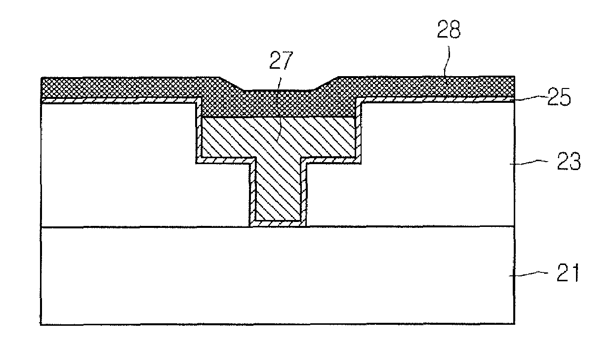
[0017]When the terms “on” or “over” are used herein, when referring to layers, regions, patterns, or structures, it is understood that the layer, region, pattern or structure can be directly on another layer or structure, or intervening layers, regions, patterns, or structures may also be present. When the terms “under” or “below” are used herein, when referring to layers, regions, patterns, or structures, it is understood that the layer, region, pattern or structure can be directly under the other layer or structure, or intervening layers, regions, patterns, or structures may also be present.
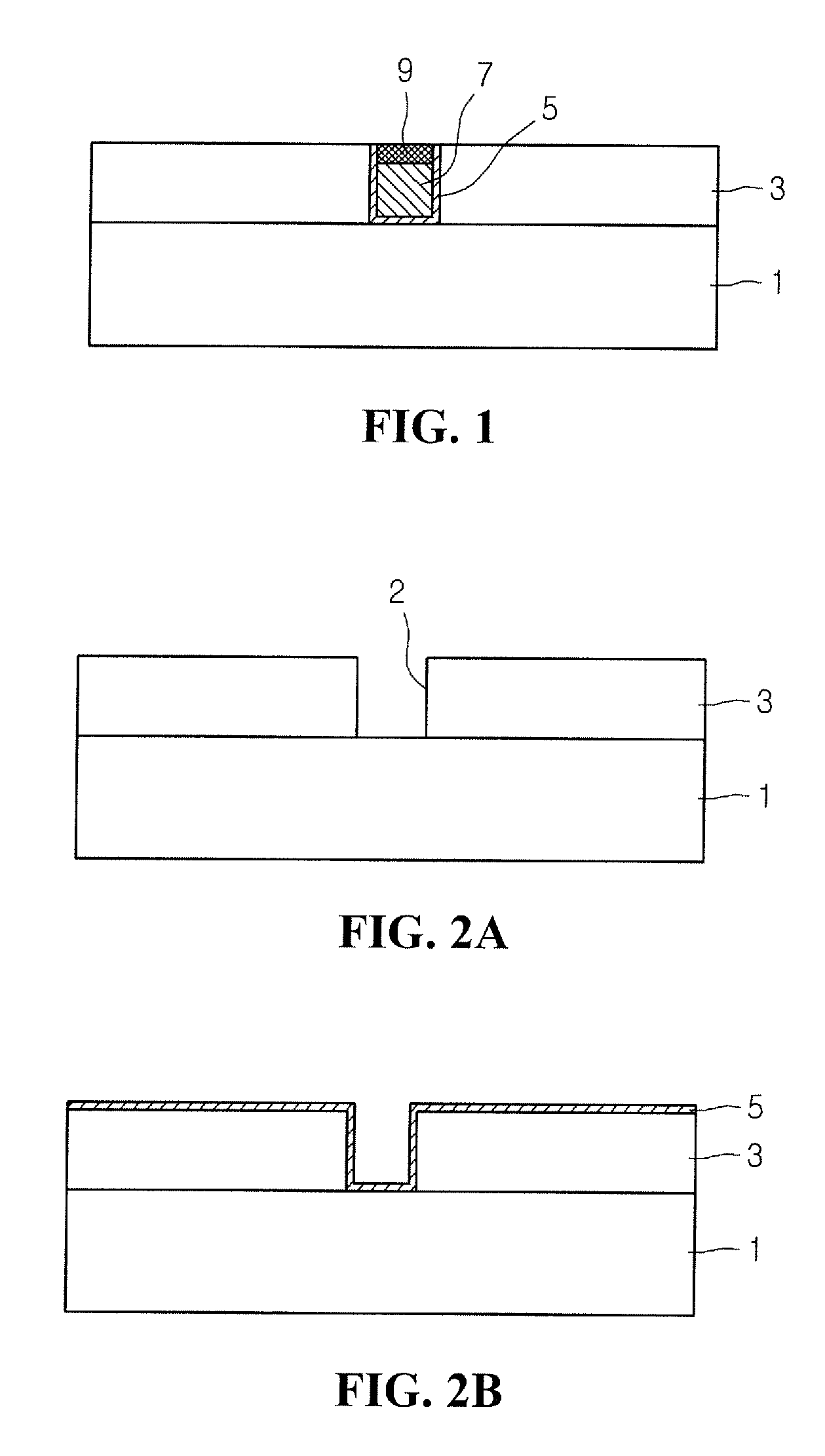
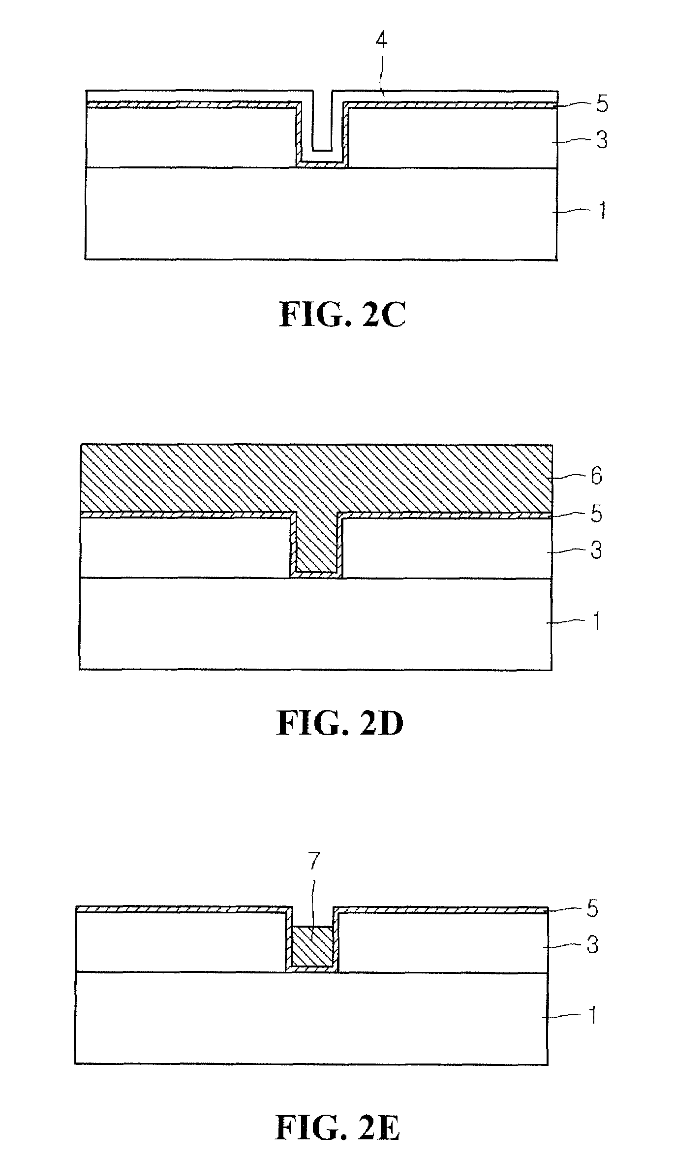
[0018]Referring to FIG. 1, a device module (not shown) having a predetermined function can be provided on a semiconductor substrate 1. The device module can be, for example, a memory or a logic circuit.
[0019]In an embodiment, an interlayer dielectric layer 3 having a via hole can be provided on the semiconductor substrate 1. In this embodiment, the interlayer dielectric layer 3 having a via hol...
PUM
 Abstract
Description
Claims
Application Information