Field effect transistor and method of fabricating same

Inactive Publication Date: 2010-01-14
GLOBALFOUNDRIES INC
View PDF14 Cites 6 Cited by
  • Summary
  • Abstract
  • Description
  • Claims
  • Application Information

AI Technical Summary

Benefits of technology

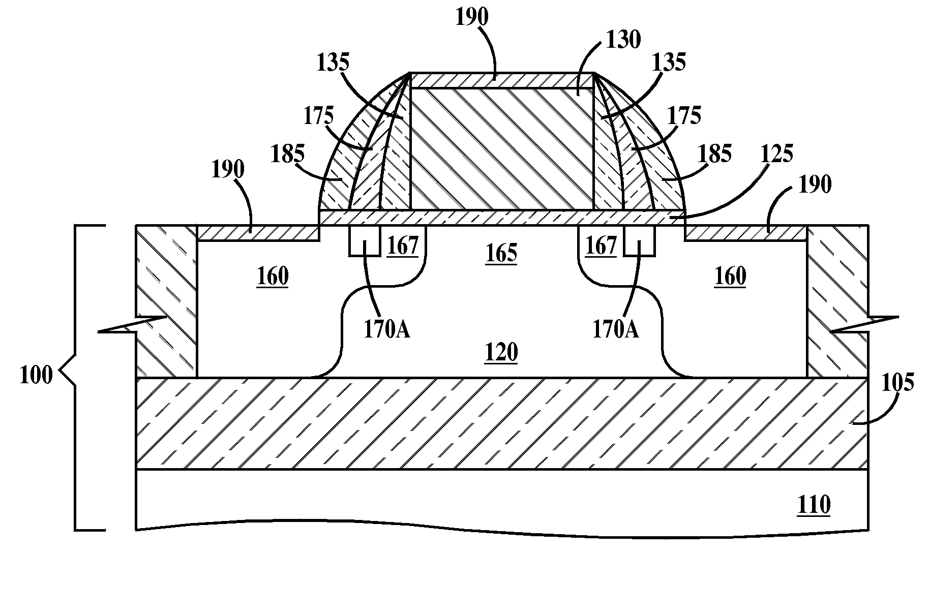
[0003]A first aspect of the present invention is a method of fabricating a field effect transistor, comprising: (a) forming a gate dielectric layer on a top surface of a silicon region of a substrate and forming a gate electrode on a top surface of the gate dielectric layer; (b) forming a source and a drain in the silicon region of the substrate on opposite sides of a gate electrode, the source and the drain separated by a channel region under the gate electrode, the source having a source (extension extending under the gate electrode and the drain having a drain extension extending under the gate electrode, the source, source extension, drain and drain extension doped a first type; and (c) forming a source delta region contained entirely within the source, a region of the source extension intervening between the source delta region and the channel region and forming a drain delta region contained entirely within the drain, a region of the drain extension intervening between the drain delta region and the channel region, the delta source region and the delta drain region doped a second dopant type, the second dopant type opposite from the first dopant type.
[0004]A second aspect of the present invention is a method of fabricating a field effect transistor, comprising: (a) forming a gate dielectric layer on a top surface of a silicon region and forming a gate electrode on a top surface of the gate dielectric layer; after (a), (b) forming first sidewall spacers on sidewalls of the gate electrode; after (b), (c) performing an angled halo ion implantation of a first dopant type and a perpendicular extension ion implantation of a second dopant type; after (c), (d) forming second sidewall spacers on the first sidewall spacers; after (d), (e) performing a perpendicular or angled source/drain ion implantation of the second dopant type; after (e), (f) performing a first activation anneal to form a source and a drain in the silicon region on opposite sides of the gate electrode, the source and the drain separated by a channel region under the gate electrode, the source having a source extension extending under the gate electrode and the drain having a drain extension extending under the gate electrode; after (e), (g) removing the second sidewall spacers; after (f) and (g), (h) performing a perpendicular counter ion implantation of the first dopant type; after (h), (i) forming third sidewall spacers on the first sidewall spacers; after (i

Problems solved by technology

As the dimensions of field effect transistors decrease, short channel effects have become a significant problem.
Short channel effects result in transistors that are more leaky than expected.

Method used


Image

  • Field effect transistor and method of fabricating same
  • Field effect transistor and method of fabricating same
  • Field effect transistor and method of fabricating same

Examples


Embodiment Construction

[0008]An angled ion implant is defined as, an implant wherein the dopant species strikes the top surface of a substrate at an incident angle of between about 6° and about 45° measured from an axis normal to the surface of the substrate. All angled ion implants described herein are performed while the substrate is rotating about an axis perpendicular to the top surface of the substrate.

[0009]A perpendicular ion implant is defined as an implant wherein the nominal incident angle of the dopant species measured from the top surface of the substrate is 90° plus or minus 3°.

[0010]An N-type dopant donates electrons to the silicon lattice while P-type dopants accept electrons from the crystal lattice, so they are opposite type dopants. Examples of N-type dopants include arsenic and phosphorous. An example of a P-type dopant is boron.

[0011]FIGS. 1A through 1O are cross-sectional drawings illustrating fabrication of a field effect transistor (FET) according to embodiments of the present inven...


PUM


Abstract

An FET and method of fabricating an FET. The method includes forming a gate dielectric layer on a top surface of a silicon region of a substrate and forming a gate electrode on a top surface of the gate dielectric layer; forming a source and a drain in the silicon region of and separated by a channel region under the gate electrode, the source having a source extension extending under the gate electrode and the drain having a drain extension extending under the gate electrode, the source, source extension, drain and drain extension doped a first type; and forming a source delta region contained entirely within the source and forming a drain delta region contained entirely within the drain, the delta source region and the delta drain region doped a second dopant type, the second dopant type opposite from the first dopant type.

Description

FIELD OF THE INVENTION[0001]The present invention relates to the field of field effect transistors; more specifically, it relates to a structure for a field effect transistor and the method of fabricating the field effect transistor.BACKGROUND OF THE INVENTION[0002]As the dimensions of field effect transistors decrease, short channel effects have become a significant problem. Short channel effects result in transistors that are more leaky than expected. Accordingly, there exists a need in the art to mitigate the deficiencies and limitations described hereinabove.SUMMARY OF THE INVENTION[0003]A first aspect of the present invention is a method of fabricating a field effect transistor, comprising: (a) forming a gate dielectric layer on a top surface of a silicon region of a substrate and forming a gate electrode on a top surface of the gate dielectric layer; (b) forming a source and a drain in the silicon region of the substrate on opposite sides of a gate electrode, the source and th...

Claims


Application Information

Patent Timeline
IPC IPC(8): H01L29/78H01L21/336
CPCH01L21/26586H01L29/1083H01L29/7833H01L29/6656H01L29/6659H01L29/665
InventorONTALUS, VIORELROBISON, ROBERT
OwnerGLOBALFOUNDRIES INC