Organic light emitting diode display

a light-emitting diode and organic technology, applied in the direction of photovoltaic energy generation, electrical equipment, semiconductor devices, etc., can solve problems such as visibility degradation, and achieve the effect of improving visibility

Active Publication Date: 2010-06-17
SAMSUNG DISPLAY CO LTD
View PDF4 Cites 58 Cited by
  • Summary
  • Abstract
  • Description
  • Claims
  • Application Information

AI Technical Summary

Benefits of technology

[0009]Accordingly, aspects of the present invention have been made to address the above-mentioned and/or or other problems occurring in

Problems solved by technology

Due to such external light reflection, the organic light emitting diode display has a pr

Method used


Image

  • Organic light emitting diode display
  • Organic light emitting diode display
  • Organic light emitting diode display

Examples


first embodiment

[0049]Hereinafter, the present invention will be described with reference to FIGS. 1 to 3.

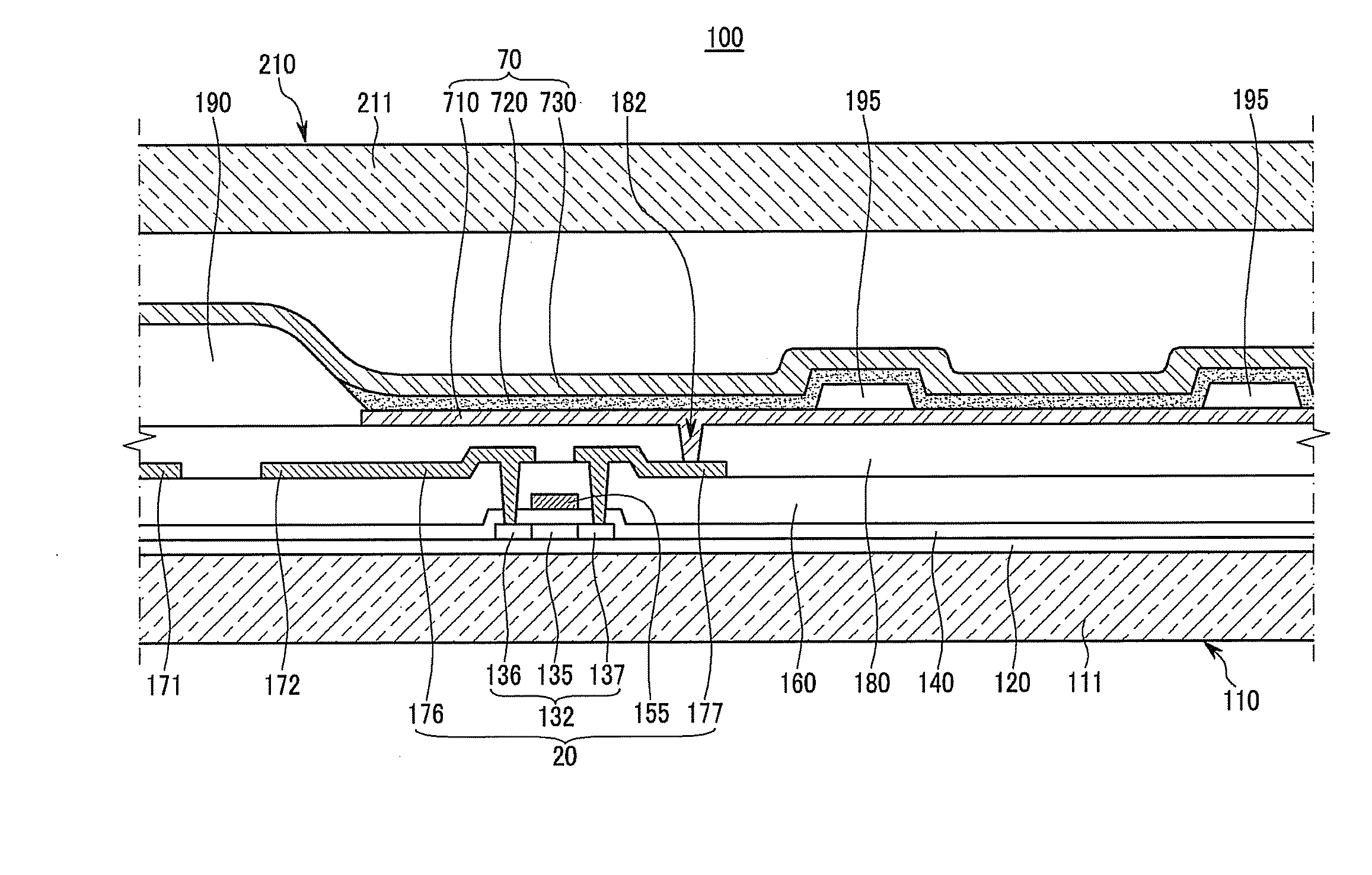
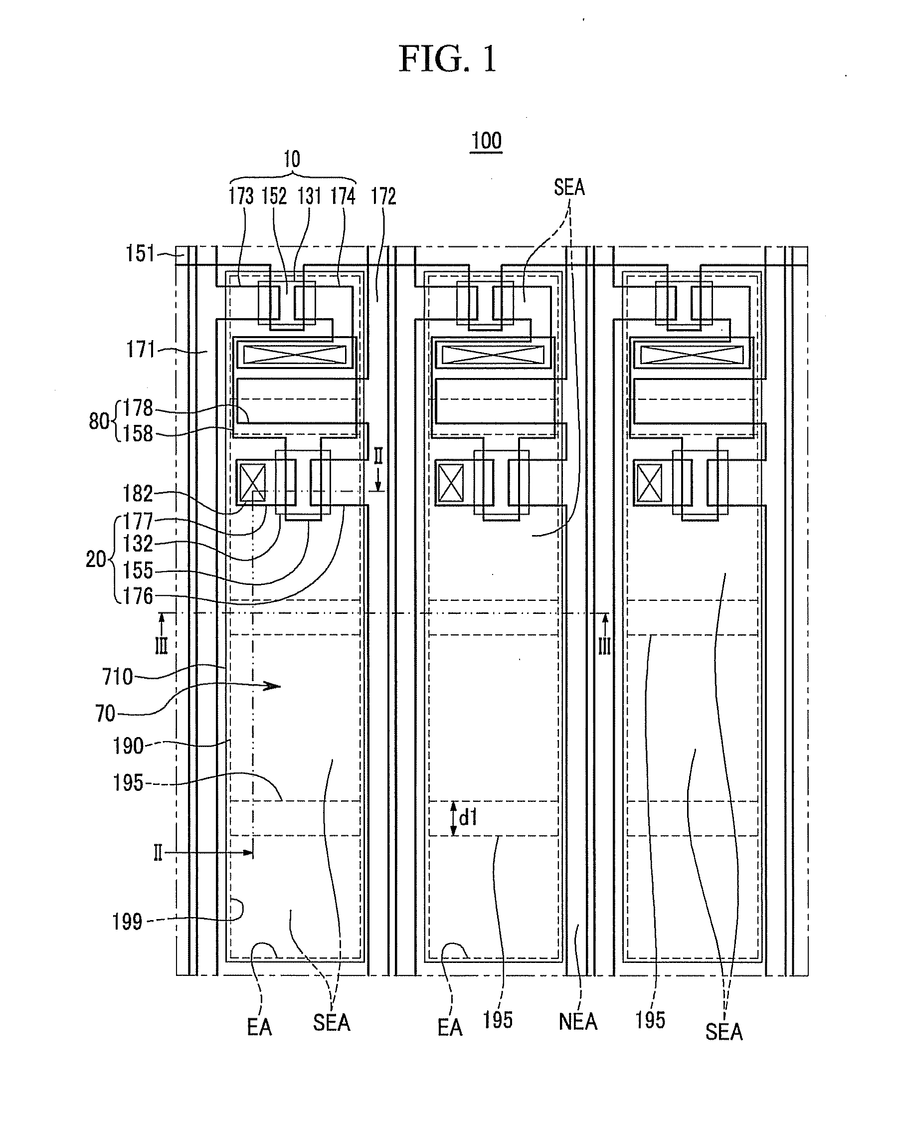
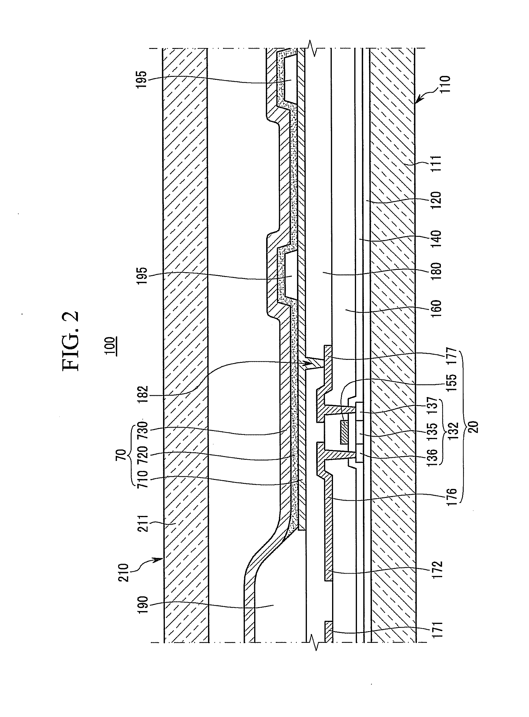
[0050]As shown in FIGS. 1 to 3, the organic light emitting diode (OLED) display 100 includes a display substrate 110 and a sealing member 210. FIG. 1 is a layout view showing the structure of a pixel on the display substrate 110. FIG. 2 is a cross-sectional view showing the display substrate 110 and the sealing member 210 taken along line II-II of FIG. 1. FIG. 3 is a cut-away perspective view of the display substrate 110 taken along line III-III of FIG. 1.

[0051]The display substrate 110 includes switching thin film transistors 10, driving thin film transistors 20, capacitors 80, and organic light emitting diodes 70 that are formed for each of pixels on a first substrate member 111. Further, the display substrate 110 includes gate lines 151 arranged in one direction, data lines 171 insulated from and crossing the gate lines 151, and a common power line 172. Here, one pixel may be defined by the ...

second embodiment

[0104]FIG. 6 shows a light shielding film pattern 222 of the sealing member 210 according to a modified example of the present invention. As shown in FIG. 6, in the modified example of the second exemplary embodiment of the present invention, the light shielding film pattern 222 of the sealing member 210 is formed in a lattice pattern. In this manner, the light shielding film pattern 222 formed in the lattice pattern can also effectively suppress external light reflection.

[0105]Hereinafter, a third exemplary embodiment of the present invention will be described with reference to FIGS. 7 and 8.

[0106]As shown in FIGS. 7 and 8, the organic light emitting diode display 300 according to the third exemplary embodiment of the present invention further includes a plurality of light scattering spacers 192 protruding on the pixel defining film 190.

[0107]The light scattering spacers 192 serve to maintain the gap between the display substrate 110 and the sealing member 210. Also, the light scat...


PUM


Abstract

An organic light emitting diode display includes: a substrate member; a pixel electrode formed on the substrate member; a pixel defining film having an opening through which the pixel electrode is exposed, and formed on the substrate member; a light absorbing layer pattern for dividing the opening into a plurality of sub-emitting areas within the opening of the pixel defining film; an organic light emitting layer formed on the pixel electrode; and a common electrode formed on the organic light emitting layer.

Description

CROSS-REFERENCE TO RELATED APPLICATION[0001]This application claims priority to and the benefit of Korean Patent Application No. 10-2008-0126039 filed in the Korean Intellectual Property Office on Dec. 11, 2008, the entire contents of which are incorporated herein by reference.BACKGROUND OF THE INVENTION[0002]1. Field of the Invention[0003]An aspect of the present invention relates to an organic light emitting diode display, and more particularly, to an organic light emitting diode display having improved visibility.[0004]2. Description of the Related Art[0005]An organic light emitting diode (OLED) display includes a plurality of light emitting diodes each having a hole injection electrode, an organic emission layer, and an electron injection electrode. An exciton is formed by combining holes and electrons inside the organic light emitting layer, and light is emitted by energy generated when the excitons fall from an excited state to a ground state, whereby the organic light emittin...

Claims


Application Information

Patent Timeline
IPC IPC(8): H01L33/00
CPCH01L27/3246H01L27/3272H01L51/5284H01L51/5281Y02E10/549H10K59/122H10K59/126H10K50/865H10K50/86H01L29/66439H10K77/10H10K50/8426
Inventor JUNG, WOO-SUKPARK, SOON-RYONGJEONG, HEE-SEONGJEONG, CHUL-WOOJEON, HEE-CHULKIM, EUN-AHKWAK, NOH-MINLEE, JOO-HWA
Owner SAMSUNG DISPLAY CO LTD
Why Eureka
Try Eureka