Active device array substrate and fabrication method thereof

a technology of active devices and array substrates, which is applied in the direction of semiconductor devices, instruments, electrical devices, etc., can solve the problems of deteriorating display quality of lcd panels, and achieve the effect of reducing display quality deterren

Active Publication Date: 2011-04-14
AU OPTRONICS CORP
View PDF3 Cites 7 Cited by
  • Summary
  • Abstract
  • Description
  • Claims
  • Application Information

AI Technical Summary

Benefits of technology

The invention provides an active device array substrate and a fabrication method that can alleviate display quality deterioration due to liquid crystal disclination. The technical effects include reducing the impact of liquid crystal disclination on display quality, improving the aperture ratio of the substrate, and reducing the size of the substrate. The fabrication method involves forming scan lines, data lines, and active devices on a substrate, followed by sequential formation of a first passivation layer, a transparent pad layer, and a second passivation layer. The color filter patterns and pixel electrodes are then formed on the second passivation layer, with a black matrix layer covering a portion of the pixel electrodes. The invention provides an improved solution for improving display quality and reducing the impact of liquid crystal disclination on display quality.

Problems solved by technology

Thereby, the display quality of the LCD panel deteriorates.

Method used


Image

  • Active device array substrate and fabrication method thereof
  • Active device array substrate and fabrication method thereof
  • Active device array substrate and fabrication method thereof

Examples


first embodiment

The First Embodiment

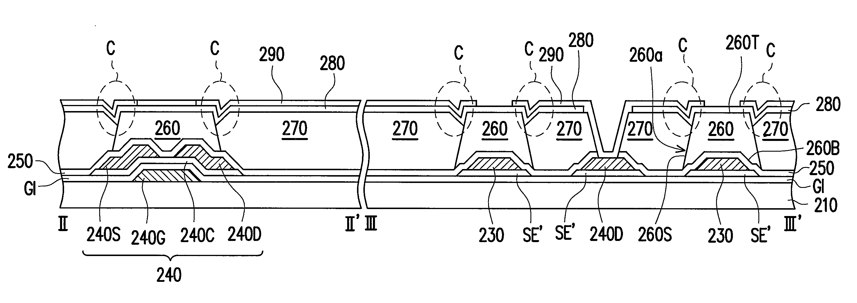
[0034]FIG. 2 is a schematic top view illustrating an active device array substrate in accordance with a first embodiment of the invention. FIGS. 3A-3H are schematic cross-sectional views illustrating a fabrication method for the active device array substrate in accordance with the first embodiment of the invention. The left sides of FIGS. 3A-3H are schematic cross-sectional views illustrating cross sections along a II-II′ line. The right sides of FIGS. 3A-3H are schematic cross-sectional views illustrating cross sections along a III-III′ line.

[0035]Referring to FIGS. 2 and 3H, an active device array substrate 200 according to the present embodiment of the invention includes a substrate 210, a plurality of scan lines 220 disposed on the substrate 210, a plurality of data lines 230 disposed on the substrate 210, a plurality of active devices 240 disposed on the substrate 210, a first passivation layer 250, a transparent pad layer(or a transparent wall) 260, a plura...

second embodiment

The Second Embodiment

[0050]FIGS. 4A-4J are schematic cross-sectional views illustrating a fabrication method of an active device array substrate in accordance with a second embodiment of the invention. The fabrication method for the active device array substrate according to the present embodiment of the invention is similar to the structure and fabrication method of the active device array substrate according to the first embodiment of the invention. A detailed description is provided hereinafter for a fabrication method of the active devices 240 according to the present embodiment of the invention.

[0051]Referring first to FIG. 4A, a first patterned conductive layer is formed on the substrate 210, wherein the first patterned conductive layer includes a plurality of scan lines 220 and a plurality of gates 240G connected to the scan lines 220. In the present embodiment of the invention, the first patterned conductive layer can further include a common line (not shown) arranged parall...


PUM


Abstract

An active device array substrate including a substrate, a plurality of scan lines, a plurality of data lines, a plurality of active devices, a first passivation layer, a transparent pad layer, a plurality of color filter patterns, a second passivation layer, a plurality of pixel electrodes, and a black matrix layer is provided. Each of the active devices is electrically connected to one of the scan lines and one of the data lines, respectively. The transparent pad layer having a plurality of openings for accommodating the color filter patterns is disposed on the first passivation layer located above the scan lines and the data lines. The first passivation layer, the color filter patterns and the second passivation layer have a plurality of contact windows therein. The black matrix layer is disposed above the transparent pad layer to cover a portion of the pixel electrodes.

Description

CROSS-REFERENCE TO RELATED APPLICATION[0001]This application claims the priority benefit of Taiwan application serial no. 98134800, filed on Oct. 14, 2009. The entirety of the above-mentioned patent application is hereby incorporated by reference herein and made a part of specification.BACKGROUND OF THE INVENTION[0002]1. Field of the Invention[0003]The invention is generally related to an active device array substrate and a fabrication method thereof. More particularly, the invention is related to an active device array substrate capable of improving liquid crystal disclination and a fabrication method thereof[0004]2. Description of Related Art[0005]With advantages of high definition, small volume, light weight, low driving voltage, low power consumption, and a wide range of applications, a liquid crystal display (LCD) panel has become the mainstream display product in the next generation. The conventional liquid crystal display panel is formed by a color filter substrate, a thin fi...

Claims


Application Information

Patent Timeline
Patent Type & AuthorityApplications(United States)
IPC IPC(8): H01L33/08H01L21/28
CPCG02F1/136209G02F2001/13373H01L27/1288H01L29/41733H01L27/1248G02F2001/136222G02F1/13373G02F1/136222
InventorTSENG, WEN-HSIENHUANG, YEN-HENGPAI, CHIA-HUICHEN, CHUNG-KAICHENG, WEI-YUANCHEN, WEN-CHUAN
OwnerAU OPTRONICS CORP