Unlock instant, AI-driven research and patent intelligence for your innovation.

Memory device and control method thereof

a memory device and control method technology, applied in the field of memory devices having nonvolatile semiconductor memory, can solve the problems of reducing file rewrite speed and increasing overhead

Inactive Publication Date: 2011-08-04
KIOXIA CORP
View PDF7 Cites 1 Cited by
  • Summary
  • Abstract
  • Description
  • Claims
  • Application Information

AI Technical Summary

Benefits of technology

The present invention provides a control method for a memory device that uses a file system that supports an incremental write method. This method includes updating a file stored in the storage area, recording an allocation table in the storage area that correlates a logical address with a virtual address and management information, and recording position information in a position information area of the storage area that represents the recording position of the management information. This allows for efficient management of files stored in the memory device and reduces the time required for updates. The invention also provides a memory device that includes a storage area and a controller that sends a logical address in response to a read request from the host, allowing for efficient management of files stored in the memory device.

Problems solved by technology

Hence, frequent occurrence of a move-write greatly increases the overhead.
For this reason, if the FAT file system is employed as a file system to manage a NAND flash memory, a move-write occurs every time cluster data is rewritten, resulting in lower file rewrite speed.

Method used


Image

  • Memory device and control method thereof
  • Memory device and control method thereof
  • Memory device and control method thereof

Examples


first embodiment

[1] Arrangement of Memory Device and Host Device

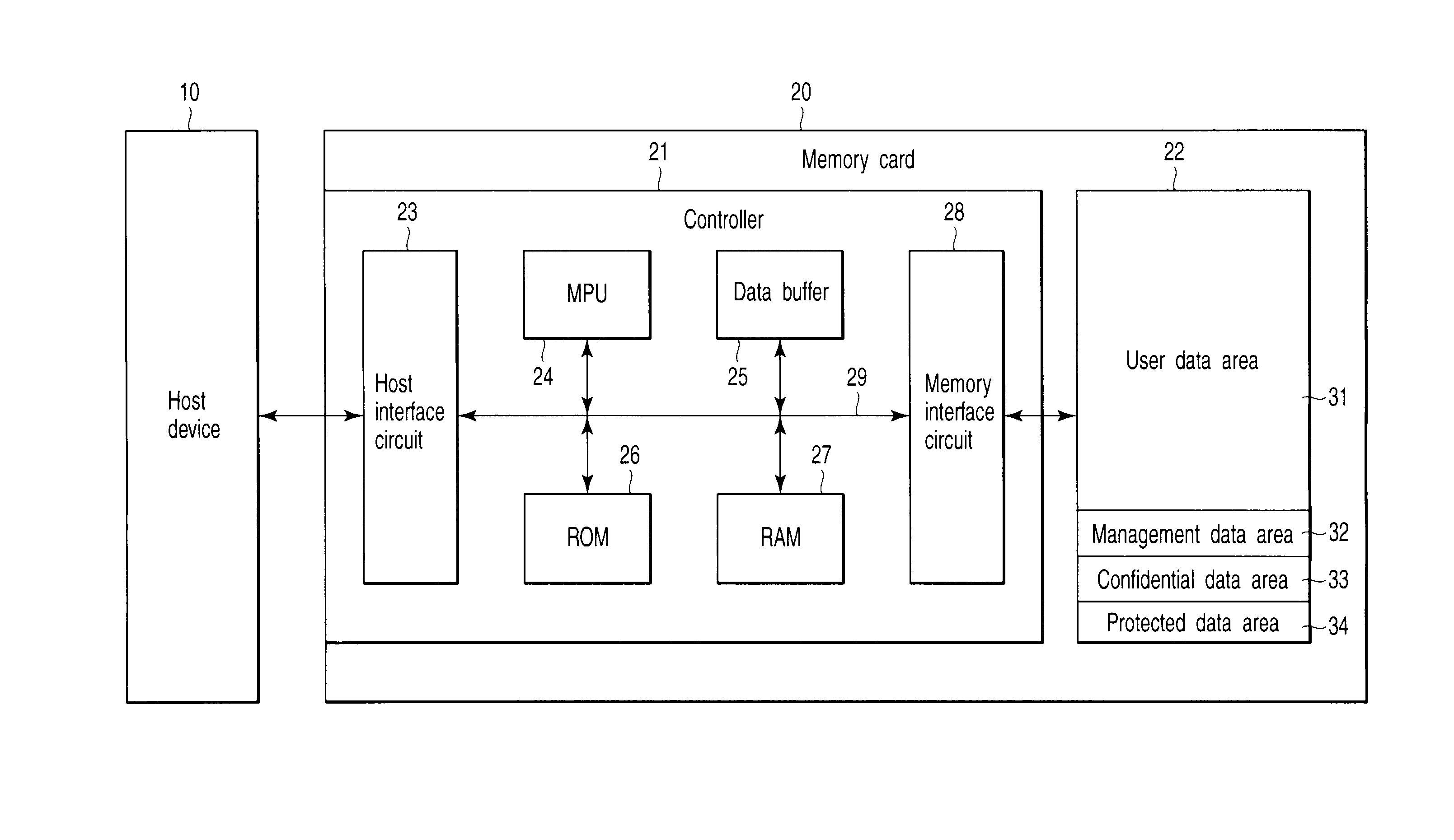
In this embodiment, a memory card will be exemplified as a memory device. A memory card is designed to be, e.g., attachable to a host device. However, the present invention is not limited to this. A memory device and a host device may be formed as one large-scale integrated circuit (LSI) or LSI package. More specifically, a controller and a nonvolatile semiconductor memory included in a memory device may be mounted on a printed circuit board with a host device.

FIG. 1 is a block diagram illustrating the arrangement of a host device 10 and a memory card 20 according to the first embodiment of the present invention. The memory card 20 is attachable to the host device 10. The memory card 20 is normally attached to the host device 10 and used as a kind of external storage medium of the host device 10.

The memory card 20 includes a nonvolatile semiconductor memory 22. In this embodiment, a NAND flash memory 22 that is a kind of electrically e...

second embodiment

FIG. 16 is a view illustrating the structure of a user data area 31 recognized by a host device 10 when a file system complying with the UDF is applied to a memory card 20 (i.e., when a flash memory 22 is formatted by the UDF). As shown in FIG. 16, the host device 10 appends data to the above-described user data area 31 of the storage areas of the memory card 20.

When the host device 10 writes data in the memory card 20 by the UDF, data are sequentially written as packets from the lower address to the higher address of the user data area 31 on the side of the memory card 20. Every time a file is updated, the VAT is updated, and the updated VAT ICB is written at the final write position. To access a written file, the host device 10 must confirm the position where the VAT ICB is written and read the VAT ICB.

When a file is repeatedly updated, a plurality of VAT ICBs are created in the user data area 31. In the example shown in FIG. 16, a file is updated twice, and accordingly, three VAT...

third embodiment

In the third embodiment, a flag is written in the redundant area of a user data area 31. VAT ICB position information is acquired by using the flag. That is, it is possible to acquire VAT ICB position information by using not a management data area 32 but only the user data area 31.

FIG. 19 is a view illustrating the structure of the physical blocks of a NAND flash memory 22. For easy understanding of the invention, the number of physical pages included in a physical block in FIG. 19 is smaller than actual. In this embodiment, the user data area 31 in the NAND flash memory 22 stores the flag to be used for searching for a VAT ICB that is normally written in the past.

Each physical page included in a plurality of physical blocks corresponding to the user data area 31 has a redundant area 35. Part (e.g., 2 bits in this embodiment) of the redundant area 35 stores a flag representing “written” or “unwritten”. There are prepared three kinds of flags: a flag (“11”) representing “unwritten” ...


PUM


Abstract

A control method of a memory device including a storage area formed of a nonvolatile semiconductor memory, includes updating a file stored in the storage area by using a file system which supports an incremental write method, recording, in the storage area, an allocation table representing a correlation between a logical address indicating a recording position of the file and a virtual address representing a virtual recording position of the file and management information of the allocation table, and recording position information representing a recording position of the management information in a position information area of the storage area.

Description

BACKGROUND OF THE INVENTION1. Field of the InventionThe present invention relates to a memory device and a control method thereof and, more particularly, to a memory device having a nonvolatile semiconductor memory and a control method thereof.2. Description of the Related ArtMemory cards including a flash memory that is as a kind of nonvolatile semiconductor memory are used as music data or video data recording media. As the file system of the memory card, for example, a file allocation table (FAT) file system is used. The FAT file system assumes a medium capable of high-speed random rewriting such as a hard disk. In random writing, data is written at random in a free sector independently of the addresses of sectors (units of write areas recognized by the file system).A typical example of a flash memory used in a memory card is a NAND flash memory. A NAND flash memory can erase data only in blocks. One block includes a plurality of write units, i.e., pages. To rewrite only part of ...

Claims


Application Information

Patent Timeline
Patent Type & Authority Applications(United States)
IPC IPC(8): G06F12/00
CPCG06F3/0611G06F3/0679G06F3/0643
Inventor ITO, TAKAFUMI
Owner KIOXIA CORP