LCD panel and fabricating method thereof
a technology of lcd panel and fabrication method, which is applied in the field of lcd panel, can solve the problems of reducing affecting the product yield of lcd panel, and causing some difficulties
- Summary
- Abstract
- Description
- Claims
- Application Information
AI Technical Summary
Benefits of technology
Problems solved by technology
Method used
Image


Examples
Embodiment Construction
[0027]The present invention will now be described more specifically with reference to the following embodiments. It is to be noted that the following descriptions of preferred embodiments of this invention are presented herein for purpose of illustration and description only. It is not intended to be exhaustive or to be limited to the precise form disclosed.
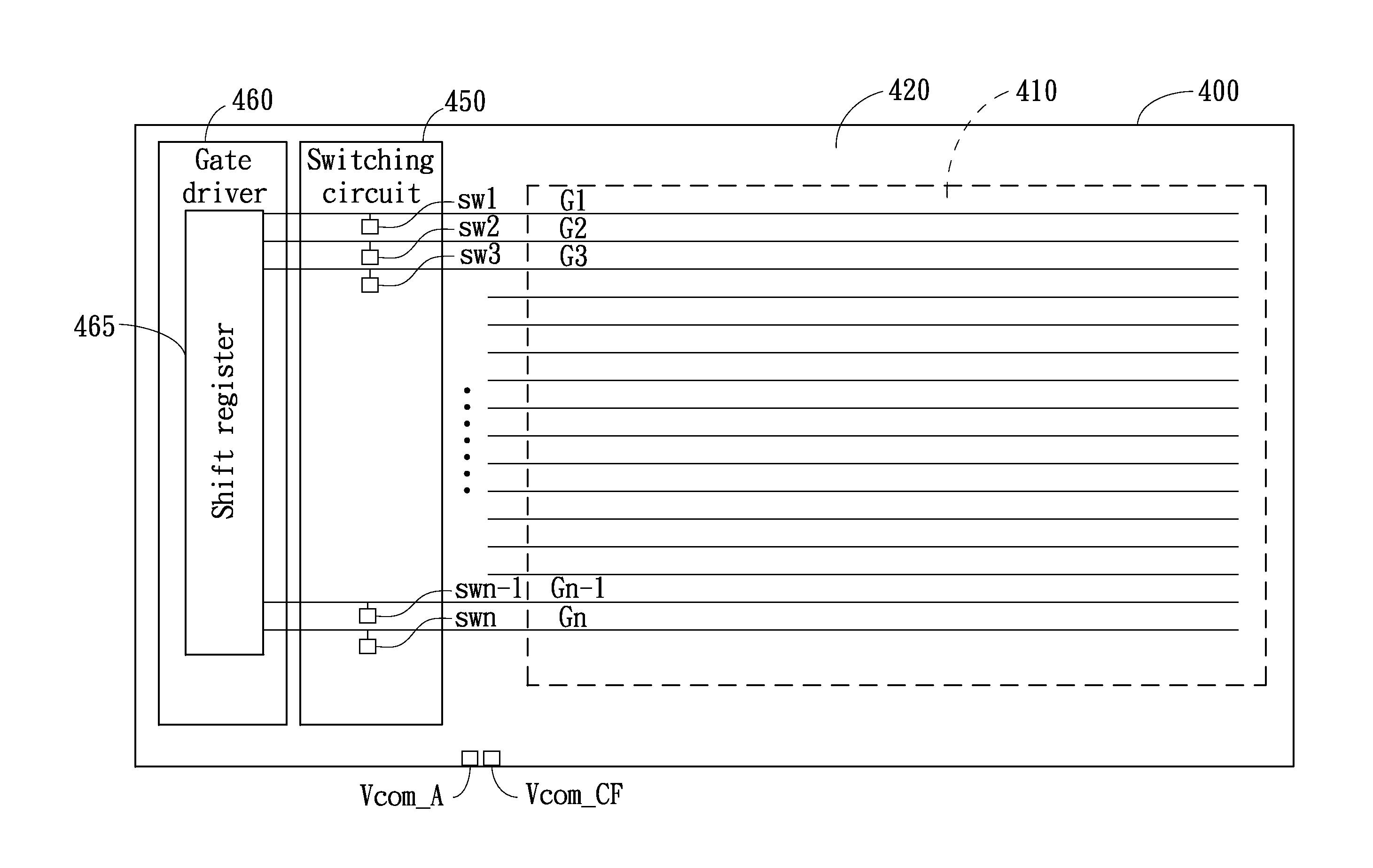
[0028]FIG. 4 is a schematic circuit diagram illustrating a shift register of a GOA substrate. The shift register 465 comprises a plurality of shift units. For clarification and brevity, only three shift units are shown in FIG. 4. Each of the shift units comprises a first transistor T1, a second transistor T2, a third transistor T3, a fourth transistor T4 and a pull-down element. Each of the shift unit is connected with a clock signal CK and an inverting clock signal XCK. Moreover, each shift unit is connected to a previous-stage shift unit.
[0029]Take the shift unit n-1 for example. The gate of the first transistor T1 of the shift...
PUM
 Abstract
Description
Claims
Application Information