System for manufacturing display unit

a display unit and manufacturing technology, applied in the direction of lamination ancillary operations, instruments, chemistry apparatus and processes, etc., can solve the problems of manufacturing apparatus and stop the carrying of optical film f, and achieve the effect of minimizing the transformation of optical film carried

US20170341360A1Active Publication Date: 2017-11-30SHANJIN OPTOELECTRONICS SUZHOU CO LTD
5 Cites 0 Cited by

Patent Information

Authority / Receiving Office
US · United States
Current Assignee / Owner
Publication Date
2017-11-30

Smart Images

  • Figure 1
    Figure 1
  • Figure 2
    Figure 2
  • Figure 3
    Figure 3
Patent Text Reader

Abstract

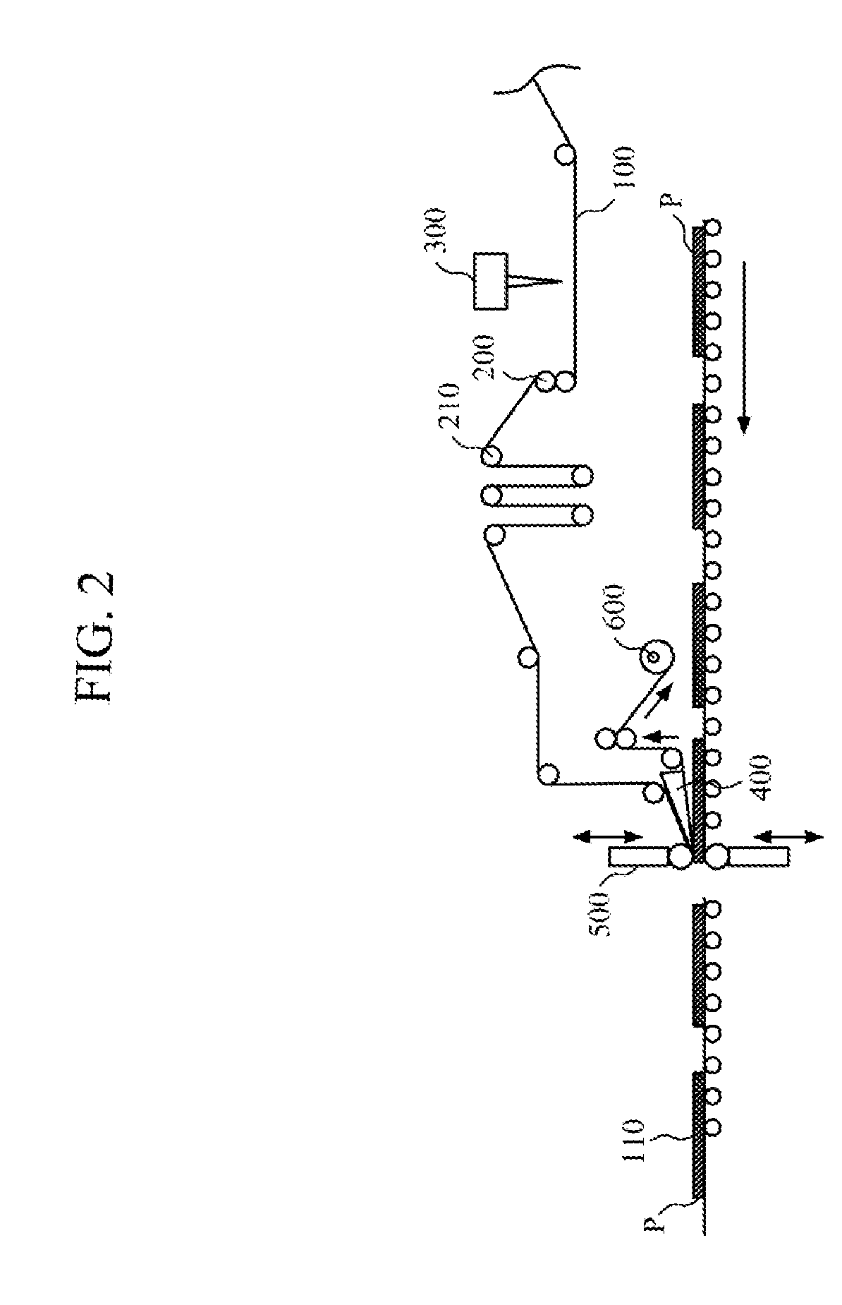
Disclosed is a system for manufacturing a display unit, including: a carrying unit configured to carry an optical film; a cutting unit configured to form a slit line on the optical film from a side opposite to the release film by a predetermined depth, in which the release film is not cut; a peeling unit configured to peel the polarizing film from the release film; and an attaching unit configured to attach the polarizing film peeled from the release film to a panel, in which the carrying unit includes a carrying direction changing unit, which changes a direction in which the optical film is carried so that the optical film carried along a first straight section is carried along a second straight section crossing the first straight section, and when the carrying of the optical film is stopped, the slit line formed on the optical film is positioned in the first straight section or the second straight section among the first straight section, the second straight section, and a curved section positioned between the first straight section and the second straight section.
Need to check novelty before this filing date? Find Prior Art

Description

TECHNICAL FIELD

[0001] The present invention relates to a system for manufacturing a display unit, and more particularly, to a system for manufacturing a display unit, which minimizes a transformation of a carried optical film when a display unit is manufactured.BACKGROUND ART

[0002] A display unit including a liquid crystal display (LCD), an organic light emitting diode (OLED), a plasma display panel (PDP), and an electrophoretic display (EPD) is manufactured through several processes. In order to manufacture the display unit, an optical film is attached onto one surface and the other surface of a panel, and when an absorption axis of the optical film attached onto one surface of the panel is vertical to an absorption axis of the optical film attached onto the other surface of the panel, the panel is normally operated. A process of attaching the optical film to the one surface of the panel will be described below.

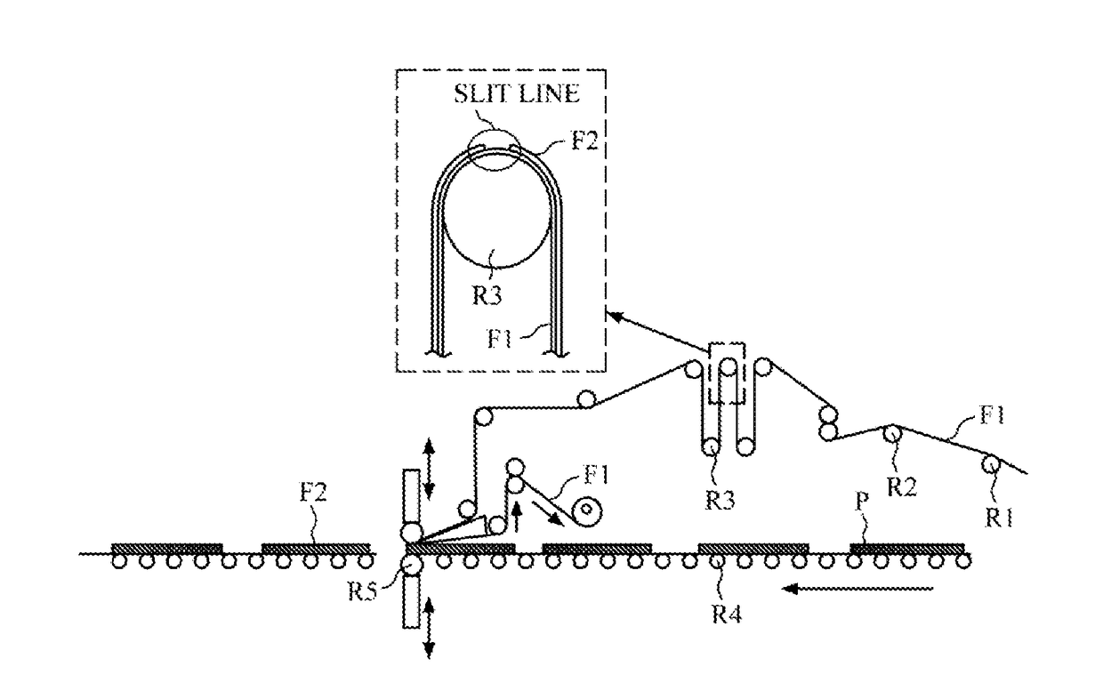
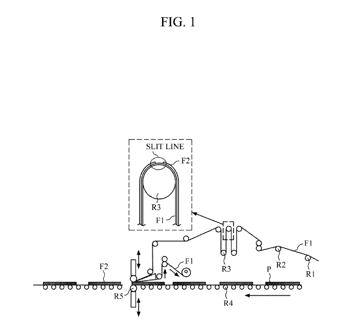
[0003] FIG. 1 is a diagram illustrating an example of a process of attachi...

Examples

Embodiment Construction

[0025]Hereinafter, the exemplary embodiments of the present invention will be described more fully with reference to the accompanying drawings so that those skilled in the art can easily carry out the present invention. However, the present invention may be modified in various different forms, are not limited to the exemplary embodiments described herein. A part irrelevant to the description will be omitted in the drawings to clearly describe the present invention, and the same elements will be designated by the same reference numerals throughout the specification.

[0026]Terms used in the present specification will be briefly described, and the present invention will be described in detail.

[0027]As the terms used in the present invention, general terms, which are currently and widely used in consideration of a function in the present invention, have been selected, but may be changed according to the intentions of those skilled in the art or judicial precedents, appearance of new tech...