Semiconductor integrated circuit

a technology of integrated circuits and semiconductors, applied in the direction of safety/protection circuits, pulse techniques, instruments, etc., can solve the problems of inefficient utilization of chip area, and achieve the effect of improving the utilization of chip area in semiconductor integrated circuits

Active Publication Date: 2018-03-29
MITSUMI ELECTRIC CO LTD
View PDF5 Cites 2 Cited by
  • Summary
  • Abstract
  • Description
  • Claims
  • Application Information

AI Technical Summary

Benefits of technology

[0006]According to at least one embodiment, the utilization o

Problems solved by technology

Such a register used in the related art is used only during the trimming mode, and is not used after the trimming

Method used


Image

  • Semiconductor integrated circuit
  • Semiconductor integrated circuit
  • Semiconductor integrated circuit

Examples


Embodiment Construction

[0018]In the following, embodiments of the present invention will be described with reference to the accompanying drawings.

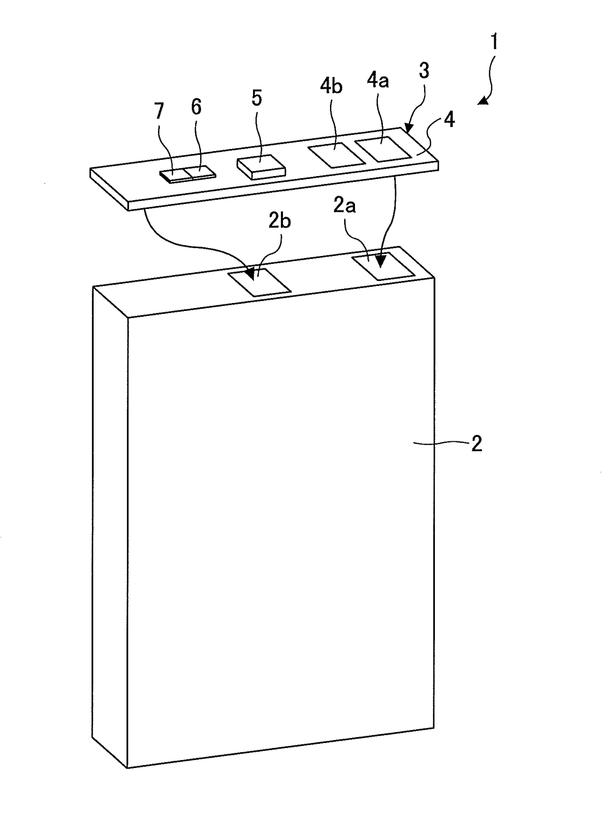
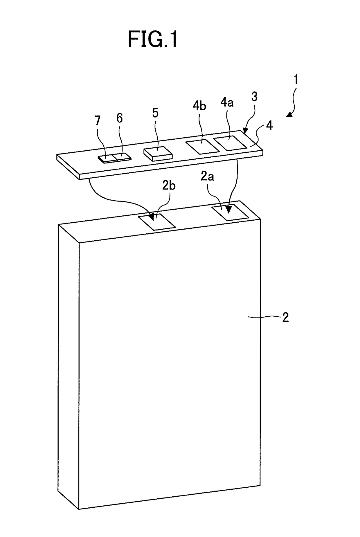
[0019]FIG. 1 is a drawing illustrating an example of the configuration of a battery pack. A battery pack 1 may be used as the power supply for a portable electronic apparatus such as a portable phone. The battery pack 1 includes a battery 2 and a battery monitoring module 3.

[0020]The battery 2 is an example of a secondary battery such a lithium ion battery. The battery monitoring module 3 includes a mounting board 4 inclusive of a printed circuit board.

[0021]The back face of the mounting board 4 has a positive-pole part connected to a positive pole 2a of the battery 2 situated on a side face thereof and a negative-pole part connected to a negative pole 2b of the battery 2 situated on the side face thereof. The front face of the mounting board 4 has load-connection terminals 4a and 4b situated on one side thereof (i.e., on the right-hand side in FIG. 1) for conne...


PUM


Abstract

A semiconductor integrated circuit includes a first circuit, a second circuit, a memory circuit having a plurality of flip-flops, a storage unit, a signal generating unit to produce an operation mode setting signal, a control circuit configured to cause the memory circuit to operate such that the plurality of flip-flops holds a value for setting characteristics of the first circuit when the operation mode setting signal indicates a first operation mode, and configured to cause the memory circuit to operate as a counter to measure a time length used in the second circuit when the operation mode setting signal indicates a second operation mode, and a setting circuit configured to cause trimming data stored in the storage unit to set the characteristic of the first circuit when the operation mode setting signal indicates the second operation mode, the trimming data corresponding to the value held by the memory circuit.

Description

BACKGROUND OF THE INVENTION1. Field of the Invention[0001]The disclosures herein relate to a semiconductor integrated circuit.2. Description of the Related Art[0002]There is a semiconductor integrated circuit known in the related art that has a register for temporarily storing trimming-purpose data in the trimming mode for correcting the variation of characteristics such as a reference voltage that may vary from product to product (see Patent Document 1, for example). The technology disclosed in Patent Document 1 keeps updating trimming-purpose data stored in the register until the reference voltage satisfies a required level. The same data as the trimming purpose data that is present in the register at the time the reference voltage satisfies the required level is then stored in a fuse unit by blowing some fuses. With this arrangement, the corrected reference voltage is produced by using the data stored in the fuse unit even after the trimming mode is disabled.[0003]Such a register...

Claims


Application Information

Patent Timeline
IPC IPC(8): G11C16/28G11C16/08G11C16/32G11C16/34
CPCG11C16/28G11C16/08G11C16/32G11C16/3454H02J7/0021H02J7/0026H01M10/425G11C29/028G11C29/023G11C7/20Y02E60/10H02J7/0031H03K3/012H03K3/037
Inventor YAMAGUCHI, TAKESHI
Owner MITSUMI ELECTRIC CO LTD
Why Eureka
Try Eureka