

Integrated circuit chip having bs-pdn structure
- Summary
- Abstract
- Description
- Claims
- Application Information
AI Technical Summary
Benefits of technology
Problems solved by technology
Method used
Image

Examples
Embodiment Construction
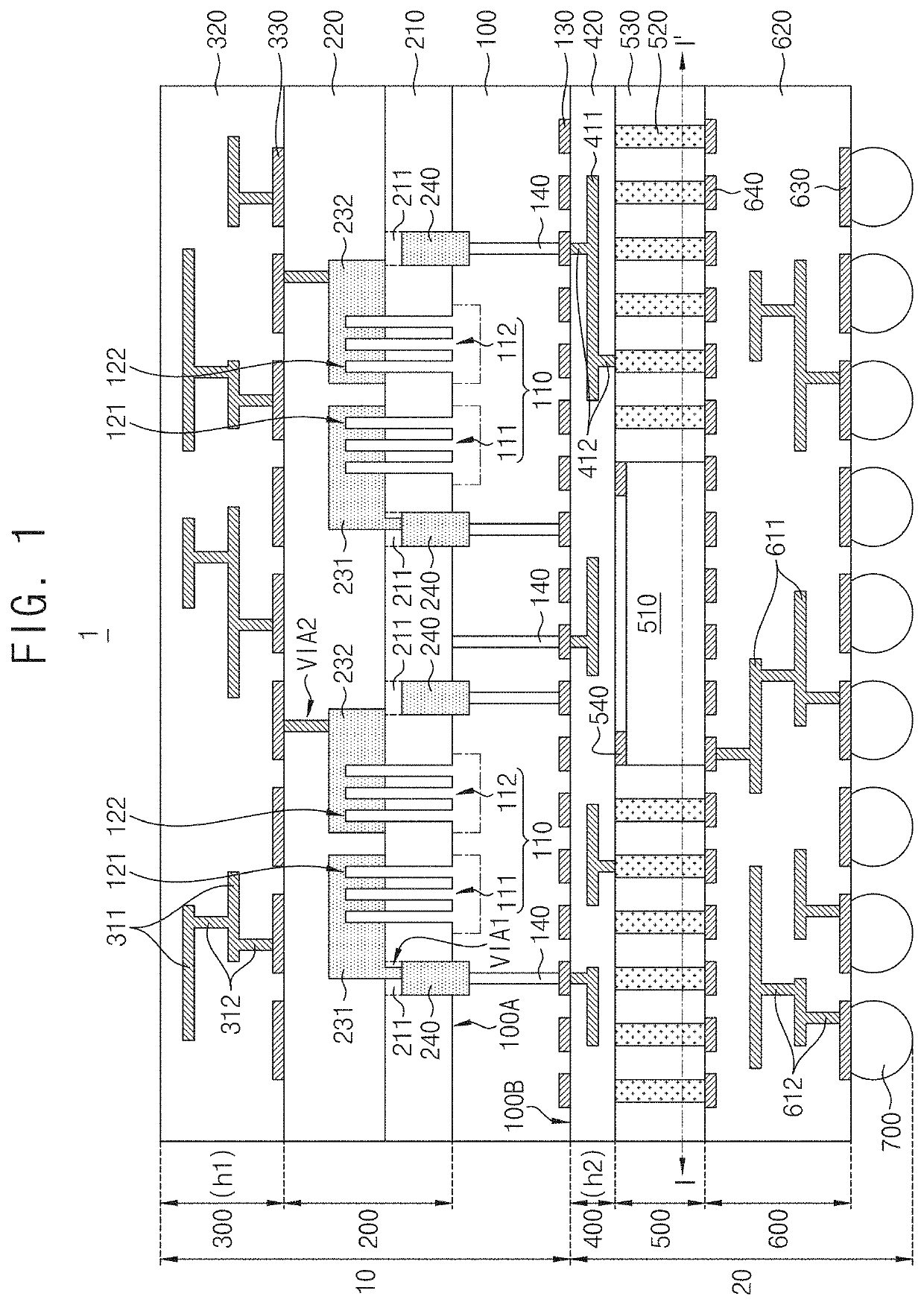
[0024]It will be understood that when an element, component, layer, pattern, structure, region, or so on (hereinafter collectively “element”) of a semiconductor device is referred to as being “over,”“above,”“on,”“below,”“under,”“beneath,”“connected to”, or “coupled to” another element of the semiconductor device, it can be directly over, above, on, below, under, beneath, connected, or coupled to the other element or an intervening element(s) may be present. In contrast, when an element of a semiconductor device is referred to as being “directly over,”“directly above,”“directly on,”“directly below,”“directly under,”“directly beneath,”“directly connected to”, or “directly coupled to” another element of the semiconductor device, there are no intervening elements present. Like numerals refer to like elements throughout this disclosure.
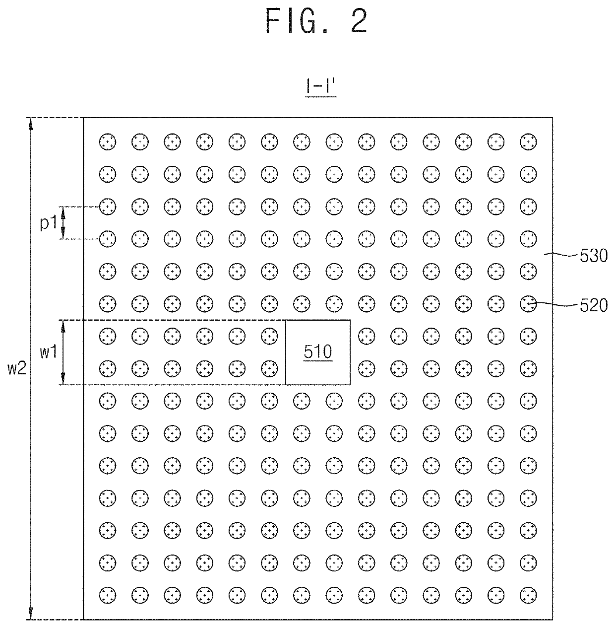
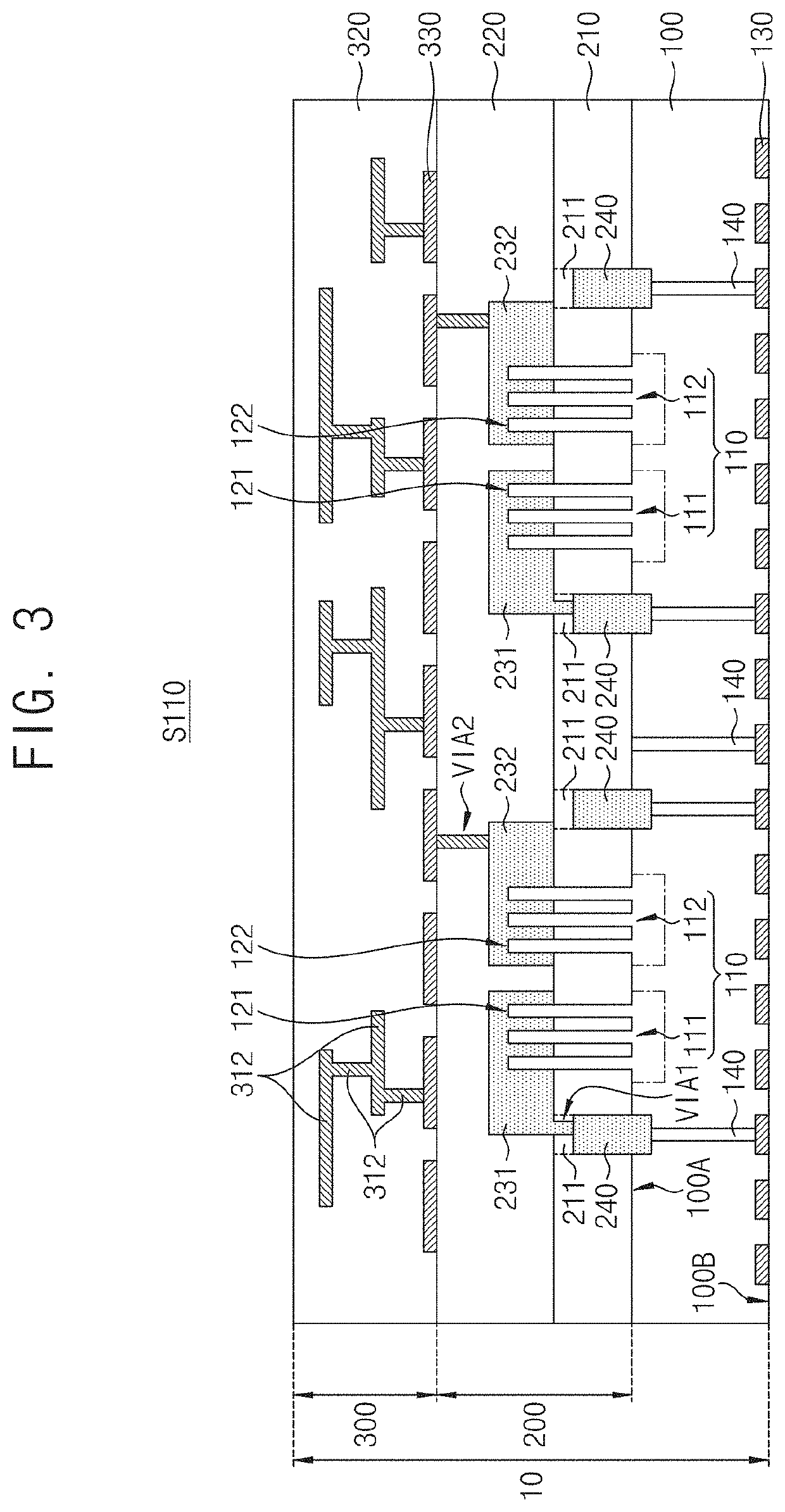
[0025]FIG. 1 is a sectional view of an integrated circuit chip according to an example embodiment of the disclosure. FIG. 2 is a plan view of a portion of...
PUM
 Abstract
Description
Claims
Application Information