Active element substrate with simplified signal line arrangement having active elements and pixel electrodes and liquid crystal display device using the same

a technology of active elements and substrates, applied in static indicating devices, instruments, optics, etc., can solve problems such as inability to simplify the structure of ladders, and achieve the effects of simplifying the arrangement of signal lines, wide process margins, and improving aperture ratio

Active Publication Date: 2007-03-27
SHARP KK
View PDF27 Cites 10 Cited by
  • Summary
  • Abstract
  • Description
  • Claims
  • Application Information

AI Technical Summary

Benefits of technology

[0023]An object of the present invention is to provide an active element substrate and a liquid crystal display device that can (i) reduce, while ensuring a wide process margin, the fluctuation of the potential of a terminal to be connected to a pixel electrode (the fluctuation of the potential occurs during OFF-period of an active element due to capacitances respectively provided by superimposing a pixel electrode on signal lines), (ii) simplify the arrangement of signal lines, and (iii) improve the aperture ratio.

Problems solved by technology

However, the ladder structure is inevitably complex, because a signal line 51 of each pixel is divided into two.

Method used


Image

  • Active element substrate with simplified signal line arrangement having active elements and pixel electrodes and liquid crystal display device using the same
  • Active element substrate with simplified signal line arrangement having active elements and pixel electrodes and liquid crystal display device using the same
  • Active element substrate with simplified signal line arrangement having active elements and pixel electrodes and liquid crystal display device using the same

Examples


Embodiment Construction

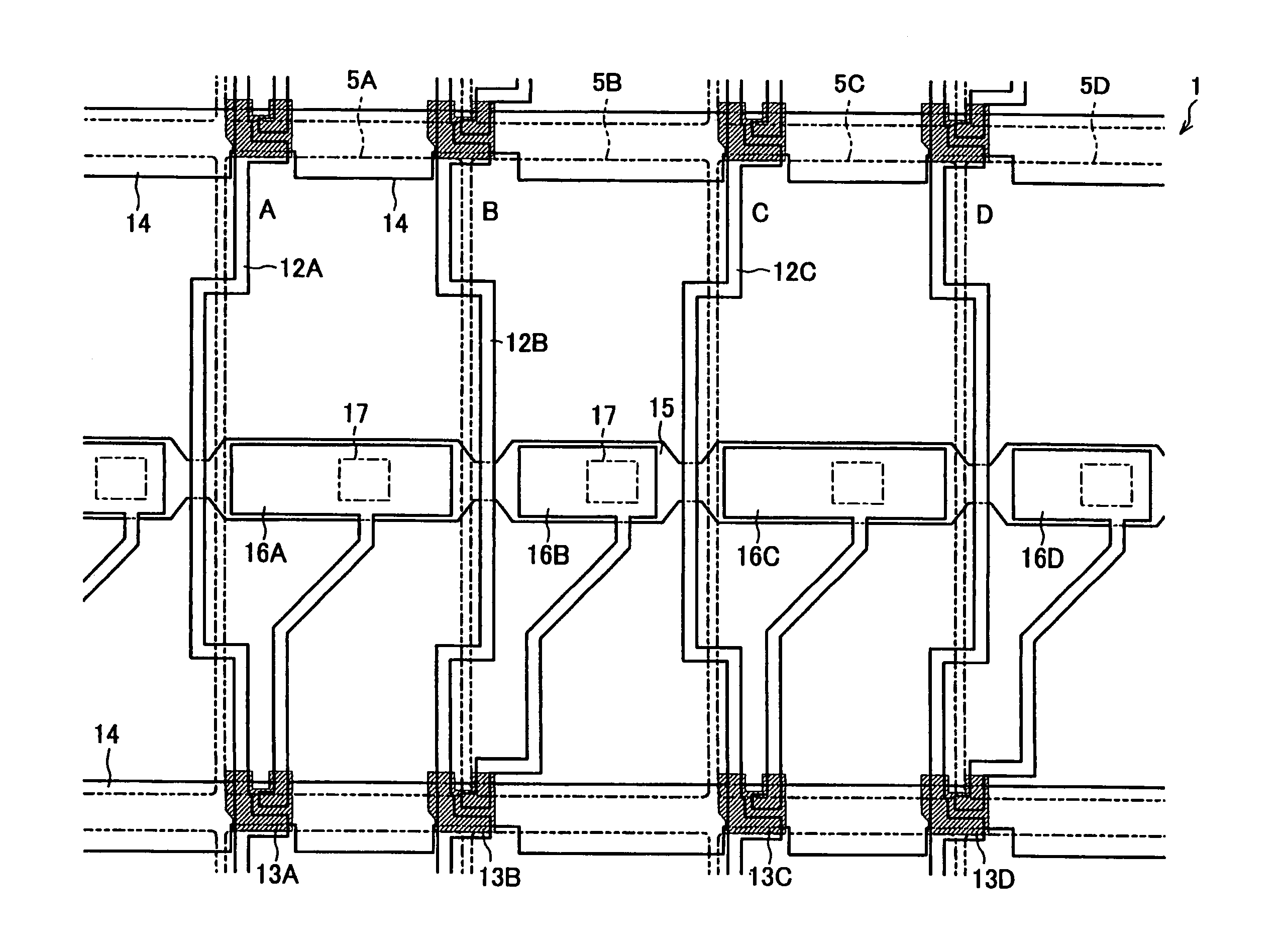
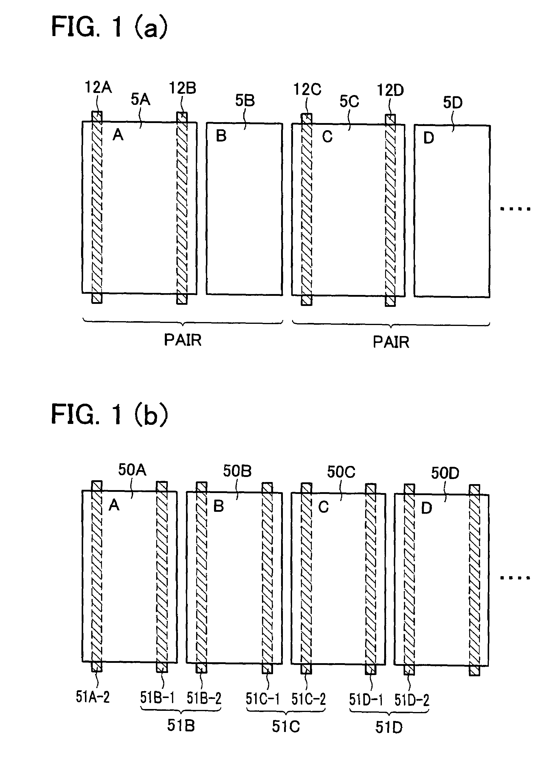
[0062]With reference to FIGS. 1 to 12, the following describes one embodiment of the present invention.

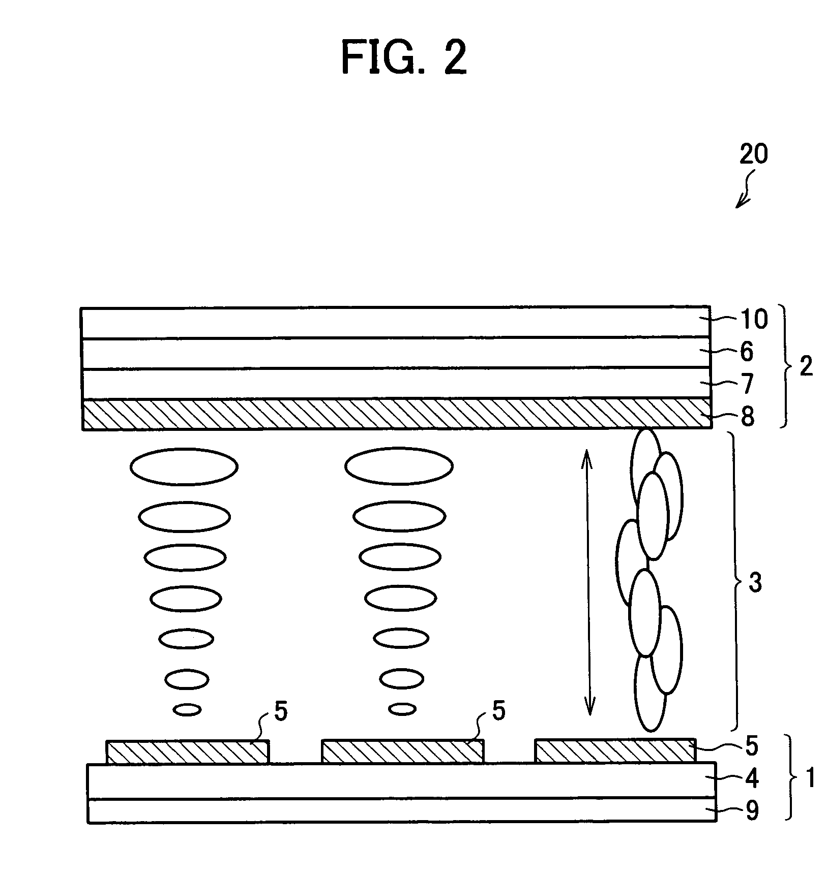
[0063]Discussed below is a case in which an active element substrate is used in a liquid crystal display device. However, the active element substrate can be used in other display devices, such as an electroluminescence display device. Moreover, the active element substrate can be used in a light-receiving device that stores charge in pixel electrodes, the charge being generated by radiation of light. An example of such a light-receiving device is an X-ray device that receives X-ray. Although the active elements used below are TFTs (thin-film transistors), other active elements (e.g. field-effect transistors, diodes) may be used instead of the TFTs. This is because, as described above, the parasitic capacitances provided by the pixel electrode and signal lines have similar influences, even if other active elements are used.

[0064]A TFT substrate (active element substrate) 1 of the f...


PUM


Abstract

An active element substrate and an opposed substrate sandwich a liquid crystal layer to constitute a liquid crystal display device. On the active element substrate, two signal lines respectively charge a pair of pixels that are adjacent to each other in a direction parallel to scanning lines. The two signal lines are provided intensively on a pixel electrode of one of the pair of pixels. In the direction parallel to the scanning lines, a pixel electrode on which signal lines are provided, and a pixel electrode on which signal lines are not provided, are arrayed alternately. This arrangement makes it possible to reduce, while ensuring a wide process margin, the fluctuation of the potential of a terminal to be connected to a pixel electrode (the fluctuation of the potential occurs during OFF-period of an active element due to capacitances respectively provided at superimposed portions of signal lines and a pixel electrode), to simplify the arrangement of signal lines, and to improve the aperture ratio.

Description

[0001]This nonprovisional application claims priority under 35 U.S.C. § 119(a) on Patent Application No. 310636 / 2003 filed in Japan on Sep. 2, 2003, and Patent Application No. 203939 / 2004 filed in Japan on Jul. 9, 2004. The entire contents of these applications are hereby incorporated by reference.FIELD OF THE INVENTION[0002]The present invention relates to an active element substrate in which each pixel is provided with an active element (e.g. a thin-film transistor, a field-effect transistor, a diode) and a pixel electrode, and relates to a liquid crystal display device using the active element substrate.BACKGROUND OF THE INVENTION[0003]In the field of liquid crystal display devices, recent trend is the widespread use of active matrix liquid crystal display devices in which each pixel has a nonlinear active element (e.g. a thin-film transistor, a field-effect transistor, a diode). This is because such active matrix liquid crystal display devices can attain excellent image quality ...

Claims


Application Information

Patent Timeline
Patent Type & Authority Patents(United States)
IPC IPC(8): G02F1/1368G02F1/1345G02F1/133G02F1/1343G02F1/1362H01L29/786
CPCG02F1/136286G02F2201/40G02F1/1368G02F1/1343
Inventor ENDA, KENJITAKEUCHI, MASANORINAGASHIMA, NOBUYOSHIKONDO, NAOFUMI
Owner SHARP KK
Why Eureka
Try Eureka