Flash memory device and method for manufacturing the same

a technology of flash memory and logic device, which is applied in the direction of semiconductor devices, electrical devices, transistors, etc., can solve the problem that the current process of the fin-type flash memory device cannot be compatible with the fin-type logic device, and achieve the effect of cost-reducing in its manufacturing and complete compatibility in the manufacturing techniqu

Active Publication Date: 2014-11-04
INST OF MICROELECTRONICS CHINESE ACAD OF SCI
View PDF20 Cites 4 Cited by
  • Summary
  • Abstract
  • Description
  • Claims
  • Application Information

AI Technical Summary

Benefits of technology

[0006]The objection of the present invention is to provide a solution to resolve at least one of the technical defects mentioned above, especially to provide a FinFET flash memory device which is compatible with FinFET device, and the manufacturing technology of the device, and at the same time, reduce the cost of manufacturing through the new method.
[0009]Complete compatibility in the manufacturing technique between the FinFET flash memory device and the FinFET logical device can be achieved as well as cost-down in its manufacturing by using the FinFET flash device and the method for manufacturing the same given by the present invention.

Problems solved by technology

However, it remains impossible for the current process of the Fin-type flash memory device to compatible with FinFET logic device.

Method used


Image

  • Flash memory device and method for manufacturing the same
  • Flash memory device and method for manufacturing the same
  • Flash memory device and method for manufacturing the same

Examples


Embodiment Construction

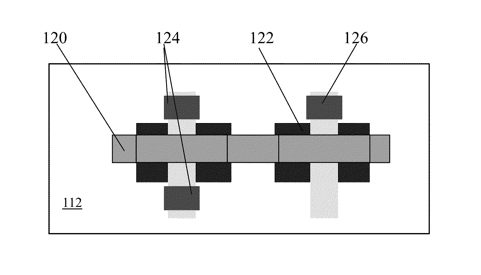
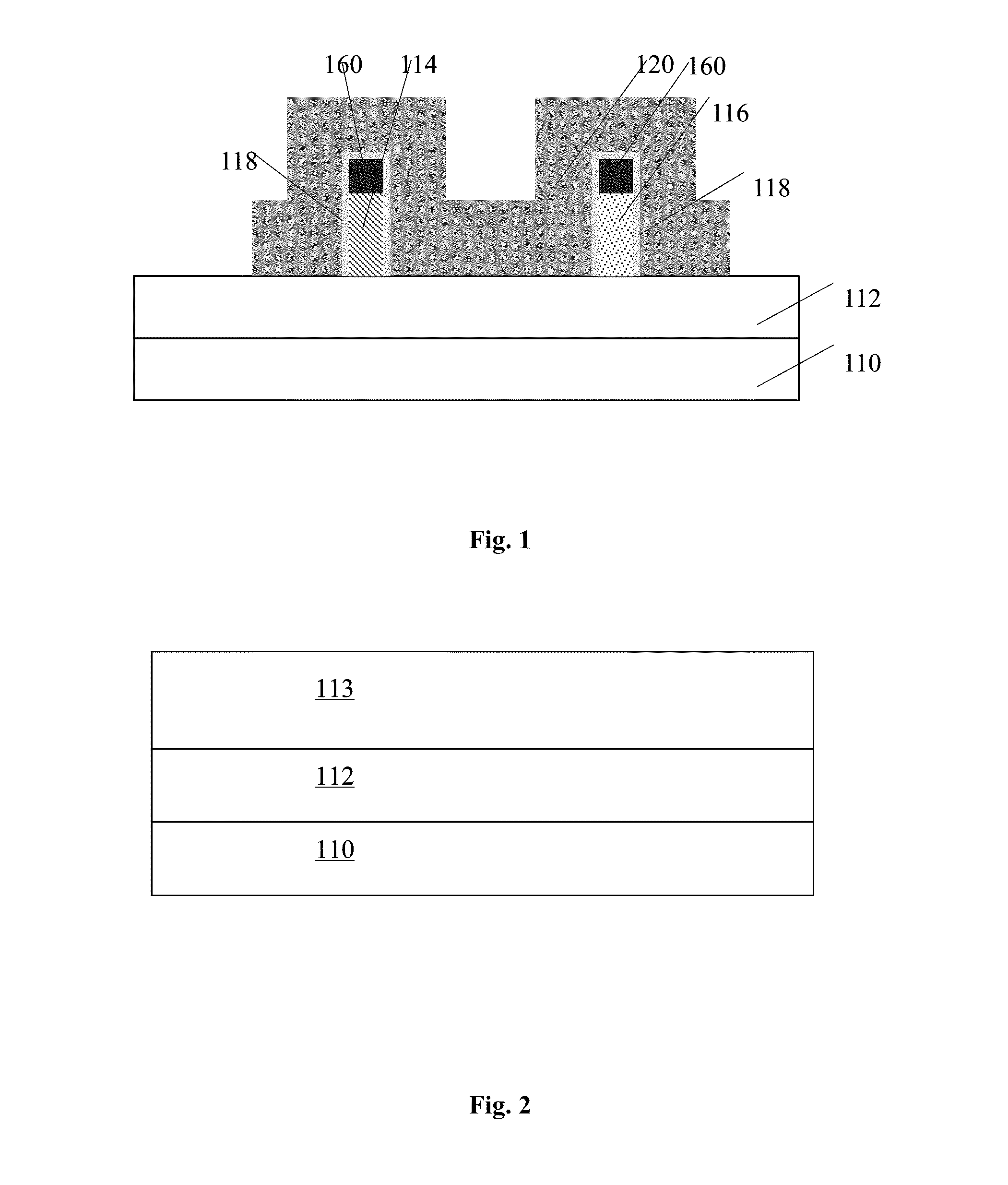
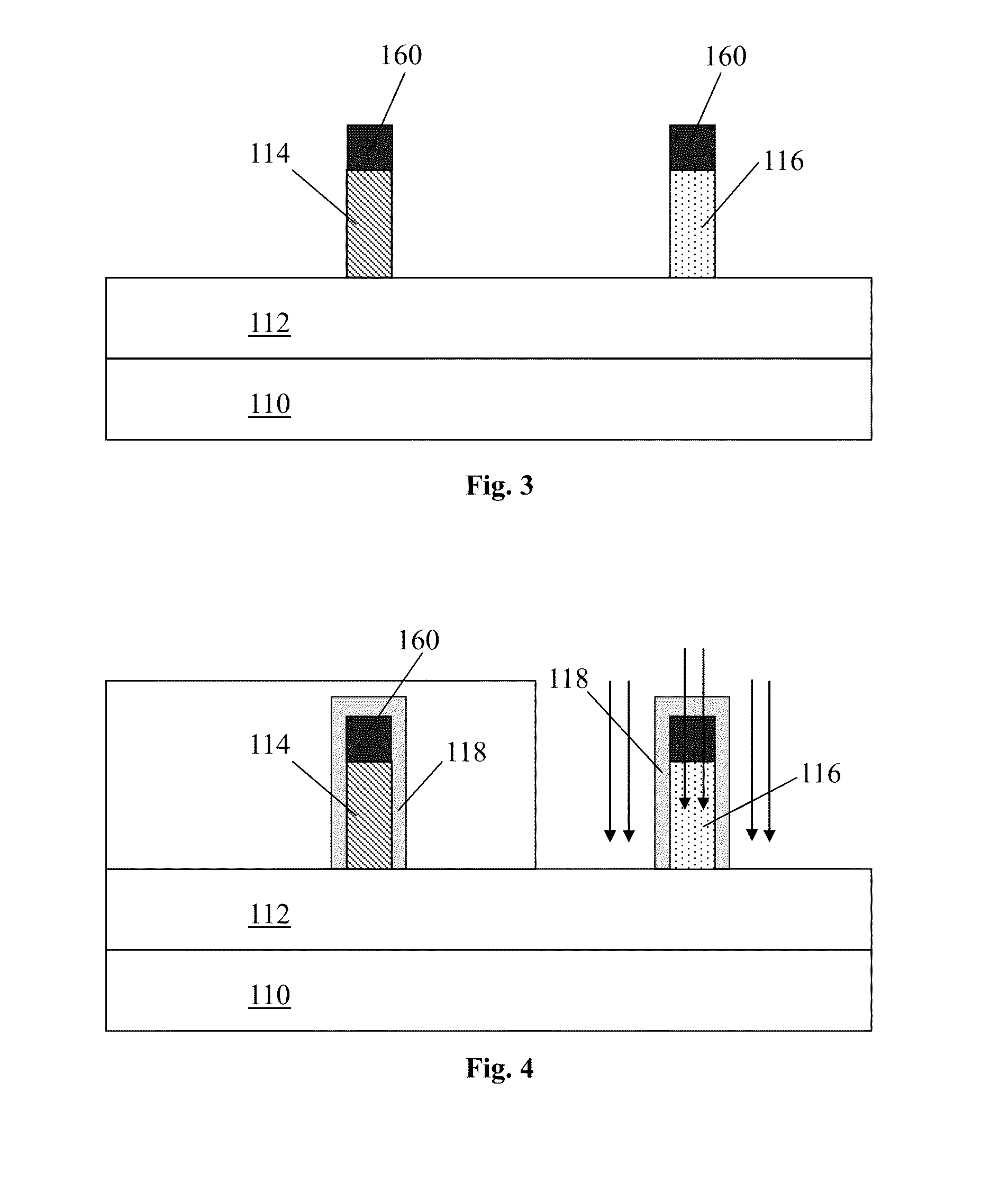
[0013]Hereunder, the present invention will be described in detail with reference to embodiments, in conjunction with the accompanying drawings.

[0014]The following disclosure will provide various embodiments or examples implementing different structure of the present invention. In order for simplification of the disclosure, devices and configurations in certain examples will be described in the following. Of course, they are only illustrative rather than limiting the present invention. In addition, figures and / or letters can be repeated in different embodiments for the purpose of simplification and clearness. However, such repetition does not indicate the relationship among various embodiments and / or configurations. Moreover, the present invention provides various examples of specific techniques and materials, but any skilled person in the art can be aware of the applicability of other techniques and / or the usage of other materials. In addition, the following description of the stru...


PUM


Abstract

The present invention provides a FinFET flash memory device and the method for manufacturing the same. The flash memory device is on an insulating layer, comprising: a first fin and a second fin, wherein the second fin is a control gate of the device; a gate dielectric layer, at side walls and top of the first fin and the second fin; source / drain regions, inside the first fin at both sides of a floating gate.

Description

CROSS REFERENCE TO RELATED APPLICATIONS[0001]The present application is a National Phase application of, and claims priority to, PCT Application No. PCT / CN2011 / 071248, filed on Feb. 24, 2011, entitled “Flash Memory Device And Method For Manufacturing The Same,” which claims the priority of Chinese Patent Application No. 201010296053.4, filed on Sep. 28, 2010. Both the PCT Application and the Chinese Application are incorporated herein by reference in their entireties.FIELD OF THE INVENTION[0002]The present invention relates to semiconductor manufacturing technology, and particularly to a flash memory device with a FinFET structure and a method for manufacturing the same.BACKGROUND OF THE INVENTION[0003]With the continuous increasing of the scale for the integrated circuits and the reduction of the size for devices, three-dimensional device has become the direction of semiconductor industry in the future development. Devices with FinFET structures have received many concerns for thei...

Claims


Application Information

Patent Timeline
Patent Type & Authority Patents(United States)
IPC IPC(8): H01L21/84H01L29/788H01L27/12H01L27/115H01L29/66
CPCH01L27/1211H01L29/66803H01L29/66825H01L21/845H01L27/11521H01L29/7881H10B41/30
Inventor ZHU, HUILONGYIN, HAIZHOULUO, ZHIJIONG
Owner INST OF MICROELECTRONICS CHINESE ACAD OF SCI
Why Eureka
Try Eureka