
Plasma processing device
A plasma and processing device technology, applied in the field of plasma processing devices, can solve the problems of increasing the standing wave effect of bipolar plates, worsening air flow uniformity, poor process results, etc., so as to reduce maintenance difficulty and maintenance time, The effect of size reduction, size reduction
Patent Information
- Authority / Receiving Office
- CN · China
- Patent Type
- Patents(China)
- Current Assignee / Owner
- Publication Date
- 2015-01-14
Smart Images
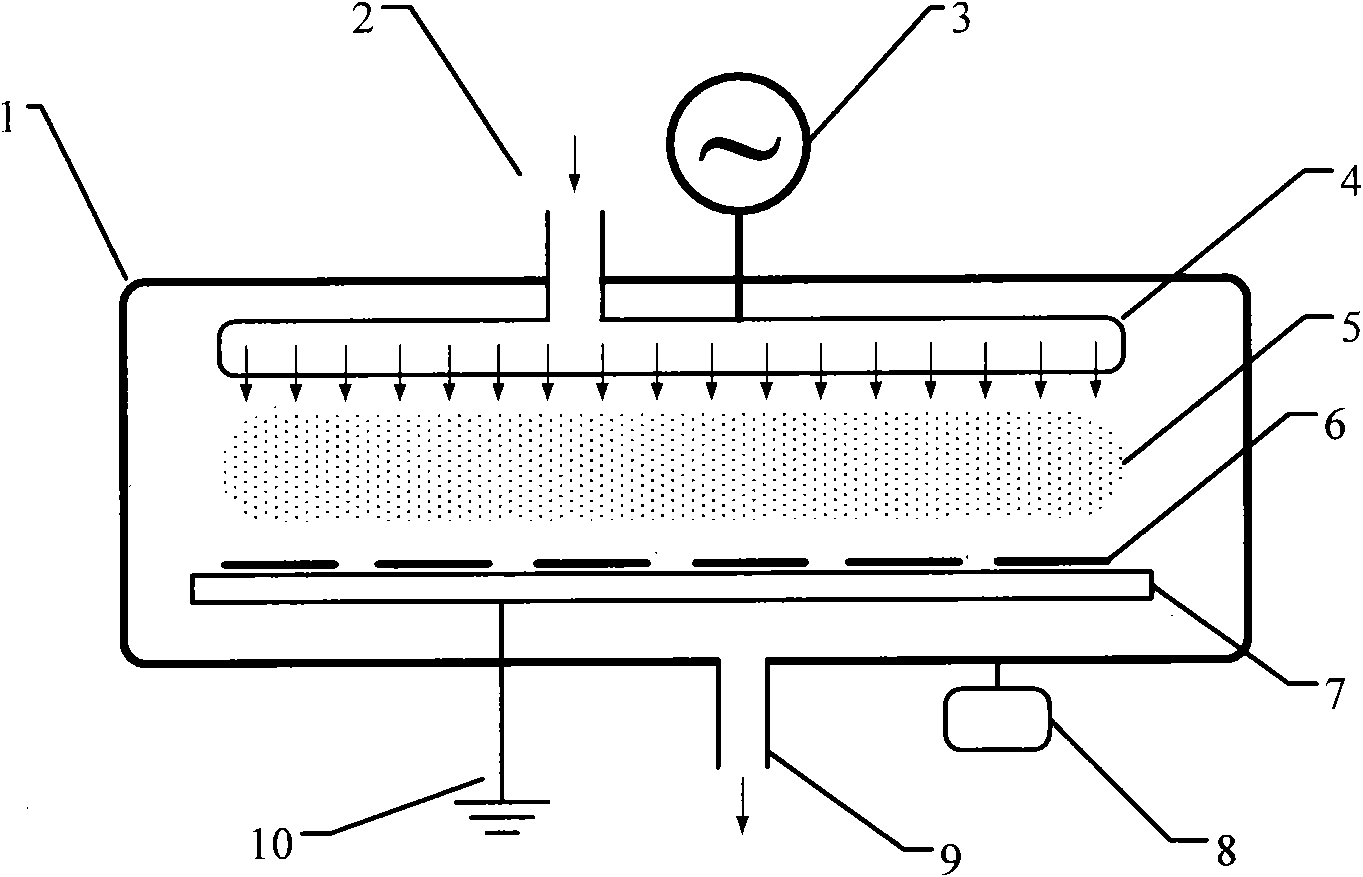
Figure 1 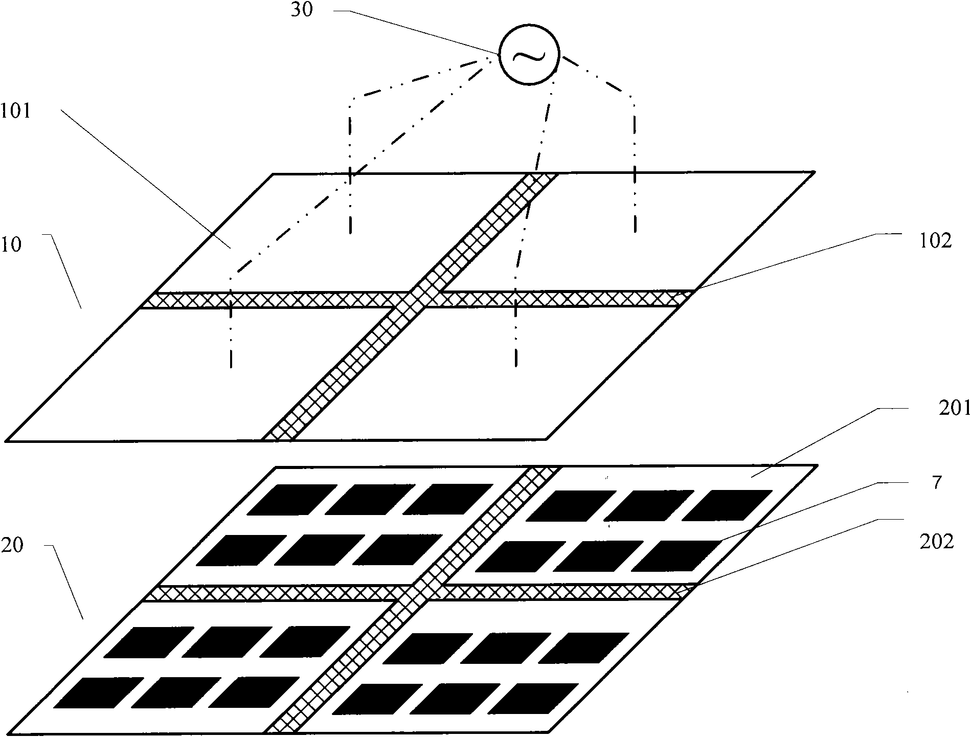
Figure 2 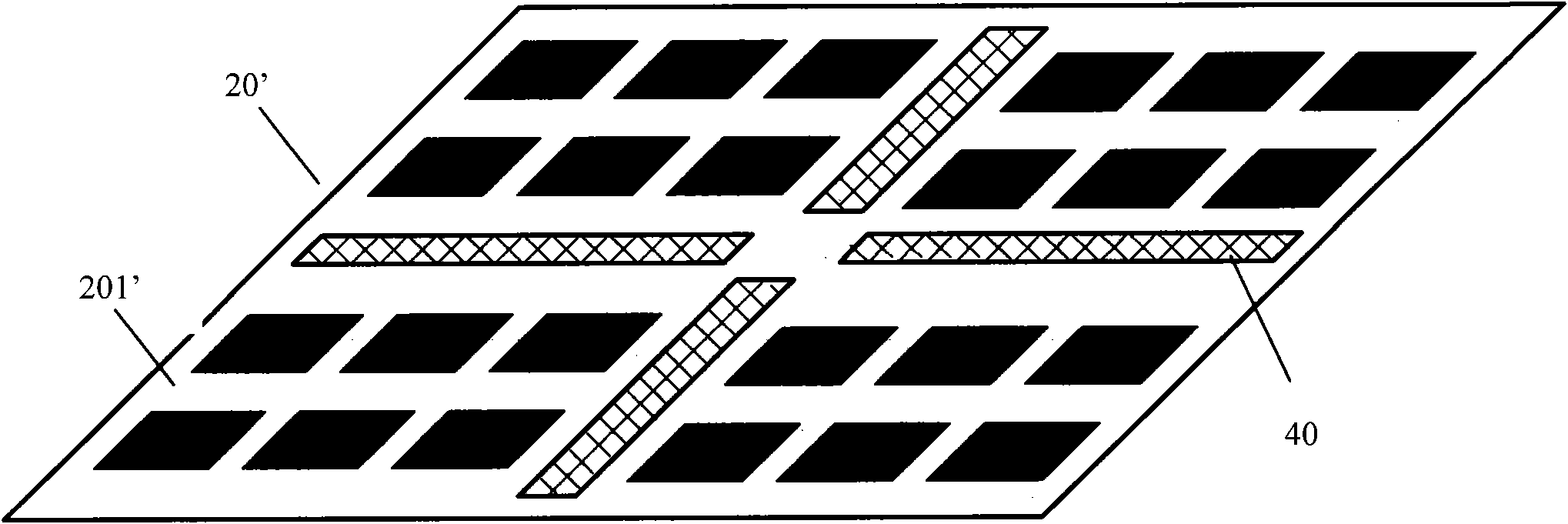
Figure 3
Abstract
Description
technical field
[0001] The invention relates to plasma processing technology, in particular to a plasma processing device. Background technique
[0002] With the continuous development of plasma (Plasma) technology, plasma processing devices have been widely used in the manufacturing process of manufacturing integrated circuits (IC) or photovoltaic (PV) products. Electron cyclotron resonance plasma (ECRP) devices, inductively coupled plasma (ICP) devices, and parallel plate capacitively coupled plasma (CCP) devices are commonly used plasma processing devices in actual production processes.
[0003] The discharge principle of the CCP device is very simple. Compared with the ECRP device and the ICP device, the generated plasma is relatively uniform. Therefore, it has been widely used in the IC industry and the PV industry.
[0004] With the continuous development of the IC and PV industries, the requirements for output rate and process results are constantly increasing, which...
Examples
Embodiment 1
[0029] figure 2 It is a schematic diagram of the plasma processing device in this embodiment. In order to clearly illustrate the inventive point of the present invention, the structure not directly related to the inventive point, such as the reaction chamber and the vacuum device, is not shown in the figure.
[0030] The plasma processing device includes: a reaction chamber (not shown in the figure), and a first pole plate 10 and a second pole plate 20 disposed opposite to each other in the reaction chamber. The first pole plate 10 is located on the upper part of the reaction chamber, and is generally called the upper pole plate. The upper pole plate is also a gas input device, which is connected with the gas channel and is used for inputting process gas into the reaction chamber. The second plate 20 is located at the lower part of the reaction chamber, commonly referred to as the lower plate, for carrying the wafer 70 to be processed. Plasma is generated in the space betwee...
Embodiment 2
[0042] This embodiment provides another plasma processing device, which differs from the first embodiment only in the structure of the second pole plate (ie, the lower pole plate). image 3 It is a schematic diagram of the second plate of the plasma processing device in this embodiment.
[0043] Such as image 3 As shown, the second pole plate 20' is not composed of a plurality of sub-plates, but a plurality of ventilation slits 40 are arranged in the pole plate, and each ventilation slit 40 divides the second pole plate into a plurality of sub-regions 201'. Each sub-region 201' and each first sub-plate 101 (see figure 2 ) correspond one-to-one.
[0044] Each of the sub-regions 201' has the same or similar shape as its corresponding first sub-plate, and their centers are aligned. In this way, the overall shape and position of each ventilation slit 40 corresponds to the gap of the first pole plate.
[0045] For example, see image 3 , each sub-area 201' is also substantia...