
Manufacturing method of semiconductor device
A manufacturing method and semiconductor technology, applied in the direction of semiconductor devices, electric solid state devices, electrical components, etc., can solve problems such as contamination of semiconductor devices
Patent Information
- Authority / Receiving Office
- CN · China
- Current Assignee / Owner
- Publication Date
- 2021-02-19
Smart Images
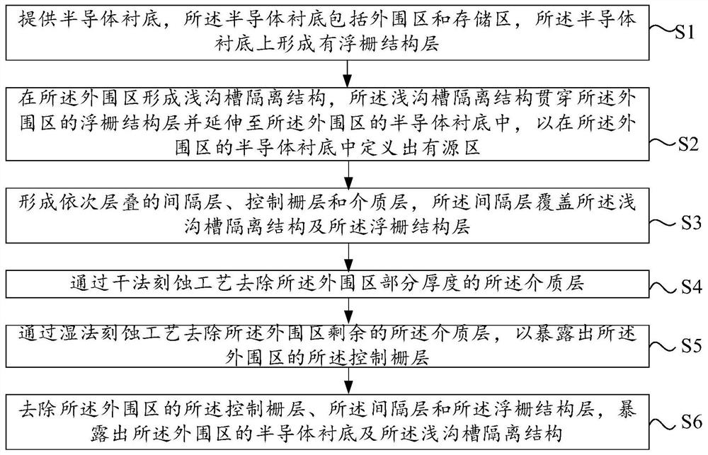
Figure 1 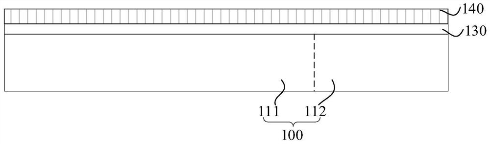
Figure 2 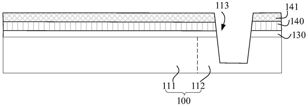
Figure 3
Abstract
Description
technical field
[0001] The invention relates to the technical field of semiconductors, in particular to a method for manufacturing a semiconductor device. Background technique
[0002] The existing manufacturing method of a semiconductor device generally includes: Step 1: providing a semiconductor substrate, the semiconductor substrate includes a storage area and a peripheral area, a shallow trench isolation structure is formed in the semiconductor substrate, and the shallow trench The isolation structure defines an active area in the semiconductor substrate, and a control gate layer and a dielectric layer are sequentially formed on the semiconductor substrate, and the control gate layer covers the shallow trench isolation structure and the semiconductor substrate; Step 2: sequentially etching the dielectric layer and the control gate layer in the peripheral area to remove the dielectric layer and the control gate layer in the peripheral area. However, in the above steps, a...
Examples
Embodiment Construction
[0038] The manufacturing method of the semiconductor device proposed by the present invention will be further described in detail below with reference to the accompanying drawings and specific embodiments. The advantages and features of the present invention will become clearer from the following description. It should be noted that all the drawings are in a very simplified form and use imprecise scales, and are only used to facilitate and clearly assist the purpose of illustrating the embodiments of the present invention.
[0039] The inventors found that, in the prior art, the reason why pits are formed in the semiconductor substrate (active region) is that when the shallow trench isolation structure is formed, the top surface of the shallow trench isolation structure is higher than the floating gate structure The top surface of the layer, after forming the spacer layer, the control gate layer and the dielectric layer stacked in sequence, the top surface of the spacer layer ...