
A waste treatment method and device suitable for PCB board production process
A production process and waste disposal technology, applied in grain processing, special data processing applications, CAD circuit design, etc., can solve the problems of wasting manpower, unable to be absorbed and cleaned, affecting the normal part of PCB processing, etc., to achieve the purpose and advantages are simple and easy understand the effect
Patent Information
- Authority / Receiving Office
- CN · China
- Patent Type
- Patents(China)
- Current Assignee / Owner
- Publication Date
- 2021-12-10
Smart Images
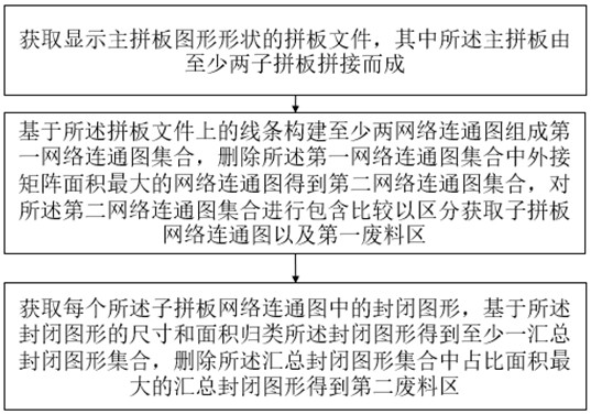
Figure 1 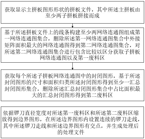
Figure 2 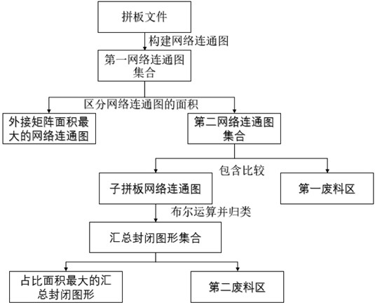
Figure 3
Abstract
Description
technical field
[0001] The present application relates to the field of big data mining, in particular to a waste treatment method and device suitable for PCB board production process. Background technique
[0002] One of the most important links from design completion to processing and manufacturing of electronic products is the processing of PCB circuit boards, and most of the bare boards processed by PCBs are assembled by placement machines, so when the size of the designed PCB board is When it is very small, in order to make small-sized PCB boards can also be placed on the placement machine for assembly, it is necessary to assemble small PCB boards; when the designed PCB size is particularly large, multiple PCB boards can also be assembled. Panel processing to obtain PCB boards of the required size, and then process the PCB boards that meet the required size according to the requirements of the customized Gerber graphics file.
[0003] In the process of PCB board process...
Examples
Embodiment 1
[0023] The embodiment of the present application provides a waste treatment method suitable for the PCB board production process, which can realize the identification of the waste area on the PCB board, and increase the routing of gongs and cutters for the excessive waste area, so that the PCB can be processed during the processing process. The purpose of crushing the oversized waste in the process. It is worth mentioning that this solution focuses on the identification of the waste area on the PCB panel. The waste area on a single PCB board is often determined, and the PCB panel includes multiple PCB sub-boards. It will take time and effort to manually identify the waste area formed between them, and the waste area on the PCB board spliced by multiple PCB sub-boards is often larger and needs to be broken up.
[0024] Specifically, refer to figure 1 and image 3 , the method includes:
[0025] Obtaining a jigsaw file showing the graphic shape of the main jigsaw, wherein t...
Embodiment 2
[0052] Based on the same idea, refer to Figure 7 , the application also proposes a waste treatment device suitable for PCB board production process, including:
[0053] The jigsaw file acquisition unit 301 is used to acquire the jigsaw file showing the graphic shape of the main jigsaw, wherein the main jigsaw is spliced by at least two sub-panels;
[0054] The first waste area acquisition unit 302 is configured to construct at least two network connected graphs based on the lines on the jigsaw file to form a first network connected graph set, and delete the network connection with the largest circumscribed matrix area in the first network connected graph set Obtaining a second set of network connectivity graphs, and performing inclusion comparison on the second set of network connectivity graphs to distinguish and obtain the sub-panel network connectivity graphs and the first waste area;
[0055] The second waste area acquiring unit 303 is configured to acquire closed figu...
Embodiment 3
[0059] This embodiment also provides an electronic device, refer to Figure 8 , including a memory 404 and a processor 402, the memory 404 stores a computer program, and the processor 402 is configured to run the computer program to perform any of the steps in any of the above embodiments of the waste treatment method applicable to the PCB board production process.
[0060] Specifically, the processor 402 may include a central processing unit (CPU), or an Application Specific Integrated Circuit (ASIC for short), or may be configured to implement one or more integrated circuits in the embodiments of the present application.
[0061]Wherein, the memory 404 may include a mass memory 404 for data or instructions. For example without limitation, the memory 404 may include a hard disk drive (HardDiskDrive, referred to as HDD), a floppy disk drive, a solid state drive (SolidStateDrive, referred to as SSD), flash memory, optical disk, magneto-optical disk, tape or Universal Serial Bus...