
Chemical vapor deposition method of integrating heating and depositing of silicon slices
A chemical vapor deposition and silicon wafer technology, applied in the field of chemical vapor deposition experiments, can solve the problems of low product efficiency, low energy utilization rate, slow temperature change, etc.
Patent Information
- Authority / Receiving Office
- CN · China
- Current Assignee / Owner
- Publication Date
- 2004-11-17
- Estimated Expiration
- Not applicable · inactive patent
Smart Images
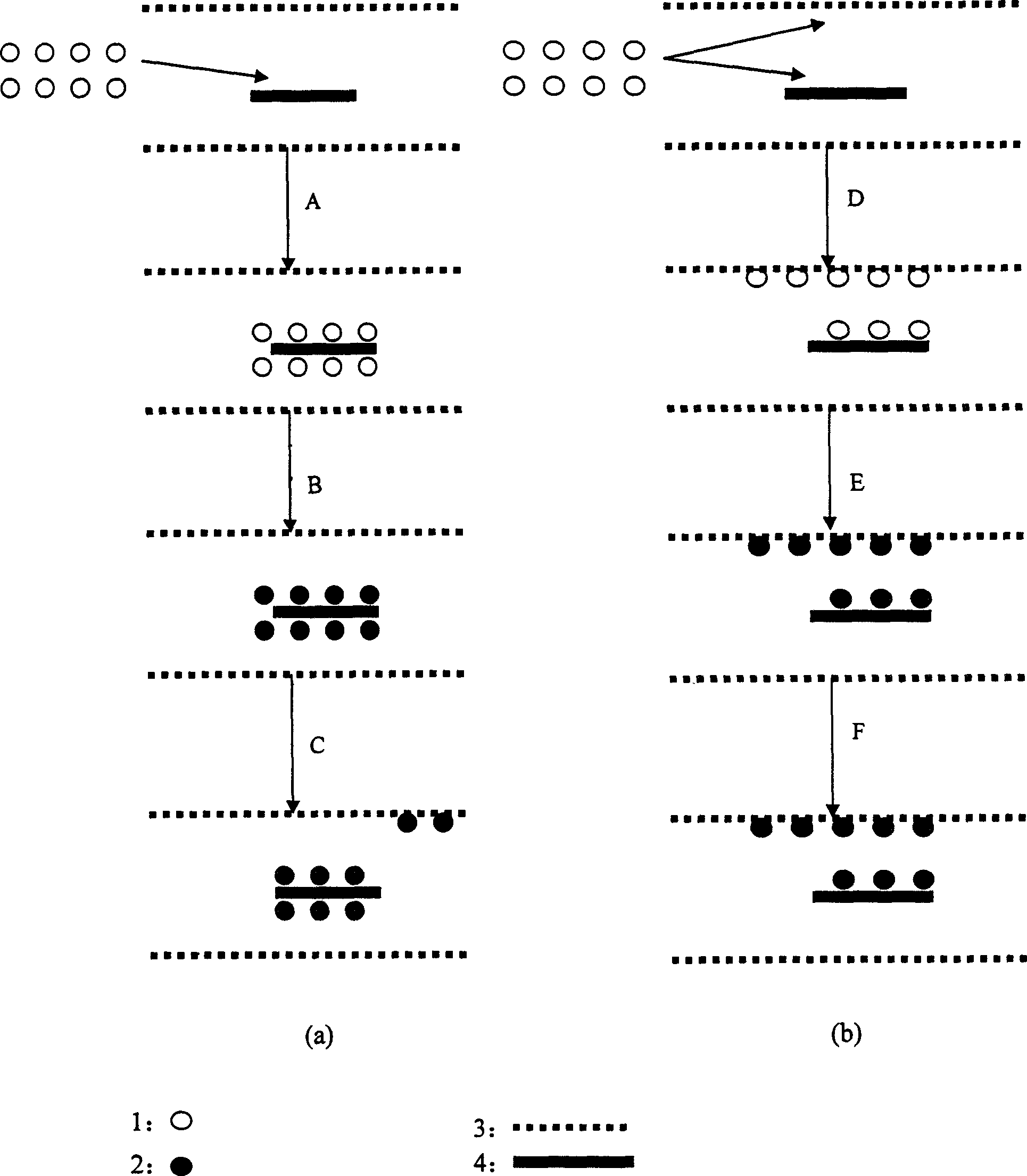
Figure 1
Abstract
Description
(1) Technical field
[0001] The invention relates to a chemical vapor deposition (CVD) experimental method integrating heating and deposition of silicon wafers. (2) Background technology
[0002] Chemical vapor deposition (CVD) is a process in which gaseous substances undergo chemical reactions on a solid surface to form solid deposits. It is a new technology for the preparation of new inorganic materials developed in the past 10 years. It has been widely used in the purification of substances, the development of new crystals, the deposition of various single crystal, polycrystalline, glassy inorganic thin films or coatings, and many other fields. In the above methods, whether it is pyrolysis reaction, chemical synthesis reaction, or chemical transport reaction, temperature control is an important condition. Many reactions are concentrated below 1200 °C, and the tube furnace is the most commonly sampled heating method. However, based on the characteristics of the design of ...
Examples
Embodiment 1
[0027] Example 1: Nano SnO on the surface of silicon wafer 2 Preparation of the array
[0028] Cut out a 20mm×5mm silicon wafer, fix it on the electrode, start the mechanical pump to evacuate, and after the vacuum is stable, start the silicon wafer micro-zone heating control device, set the temperature at 800°C, and use carbon tetrachloride gas as the Buffer, slowly pass into SnH 4 After the reaction is over, turn off the power supply of the silicon wafer micro-zone heating control device and the power supply of the mechanical pump, and take out the silicon wafer. SnO can be obtained on the surface of the silicon wafer 2 nanoarray. The arrays are neatly arranged and numerous in number, like continuous rice seedlings in an electric environment. control of different SnH 4 Depending on the gas concentration and the temperature of the silicon wafer, nanoparticles of various shapes such as chrysanthemum can be obtained.
Embodiment 2
[0029] Embodiment 2: Mo on the surface of silicon wafer 2 o 3 Fabrication of nanoribbons
[0030] Cut out a 20mm×5mm silicon wafer, fix it on the electrode, start the mechanical pump to evacuate, and after the vacuum is stable, start the silicon wafer micro-zone heating control device, set the temperature at 1000°C, and place the metal molybdenum powder on the silicon The surface of the wafer is heated, vaporized and deposited (it can be placed on the surface of the silicon wafer before vacuuming). After the reaction is completed, turn off the power supply of the silicon wafer micro-zone heating control device and the power supply of the mechanical pump, and take out the silicon wafer. The molybdenum oxide nanobelt can be obtained, and the ratio of the length, width and thickness of the ribbon is about 100:10:1 when observed under electric conditions. In addition, many other shapes of nanomolybdenum oxide particles were obtained.
Embodiment 3
[0031] Embodiment 3: Preparation of nano-gold particles on the surface of silicon wafer (extended application of the present invention)
[0032] Porous silicon is required for the preparation of traditional gold nanoparticles on the surface of silicon wafers, but it is not easy to make porous silicon from directly purchased single crystal silicon wafers (non-porous silicon). This method utilizes the characteristic of rapid temperature change of the new heating technology, first sprays gold on the surface of a 5mm×20mm silicon wafer, then fixes the silicon wafer on the electrode, starts the silicon wafer micro-zone heating controller power supply, and sets the temperature at 1100°C After reaching the temperature, cut off the power supply, quickly cool down and anneal the silicon wafer, and then obtain 20-100nm gold particles on the surface of the silicon wafer, and the gold particles are evenly distributed and not connected to each other. By controlling the thickness and anneal...