
Method of providing reacted metal source-drain stressors for tensile channel stress
a tensile channel and stressor technology, applied in the direction of semiconductor devices, electrical equipment, semiconductor/solid-state device details, etc., can solve the problems of void formation, reduced stress achievable by this mechanism, and more than the channel material of silica, so as to reduce or eliminate the diffusion into the channel, the contact resistance is low, and the effect of easy formation of metal sd
Patent Information
- Authority / Receiving Office
- US · United States
- Patent Type
- Patents(United States)
- Current Assignee / Owner
- Publication Date
- 2019-12-17
Smart Images
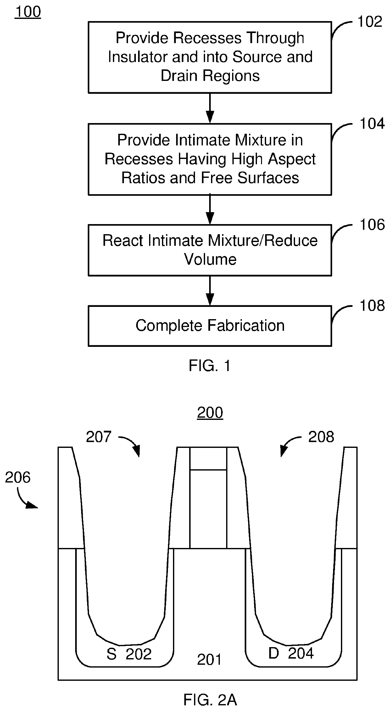
Figure 1 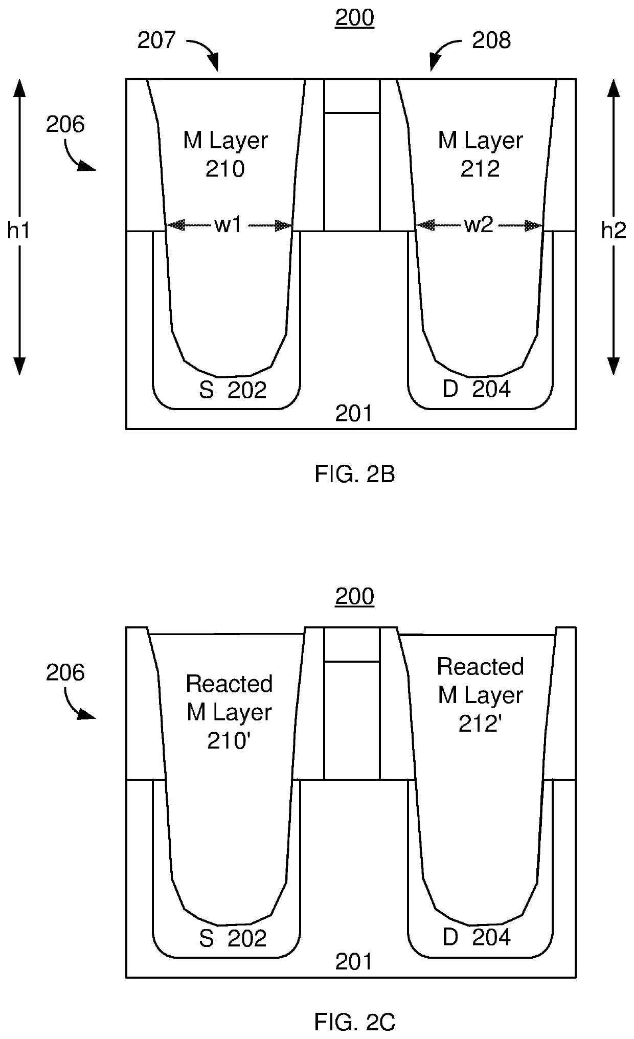
Figure 2 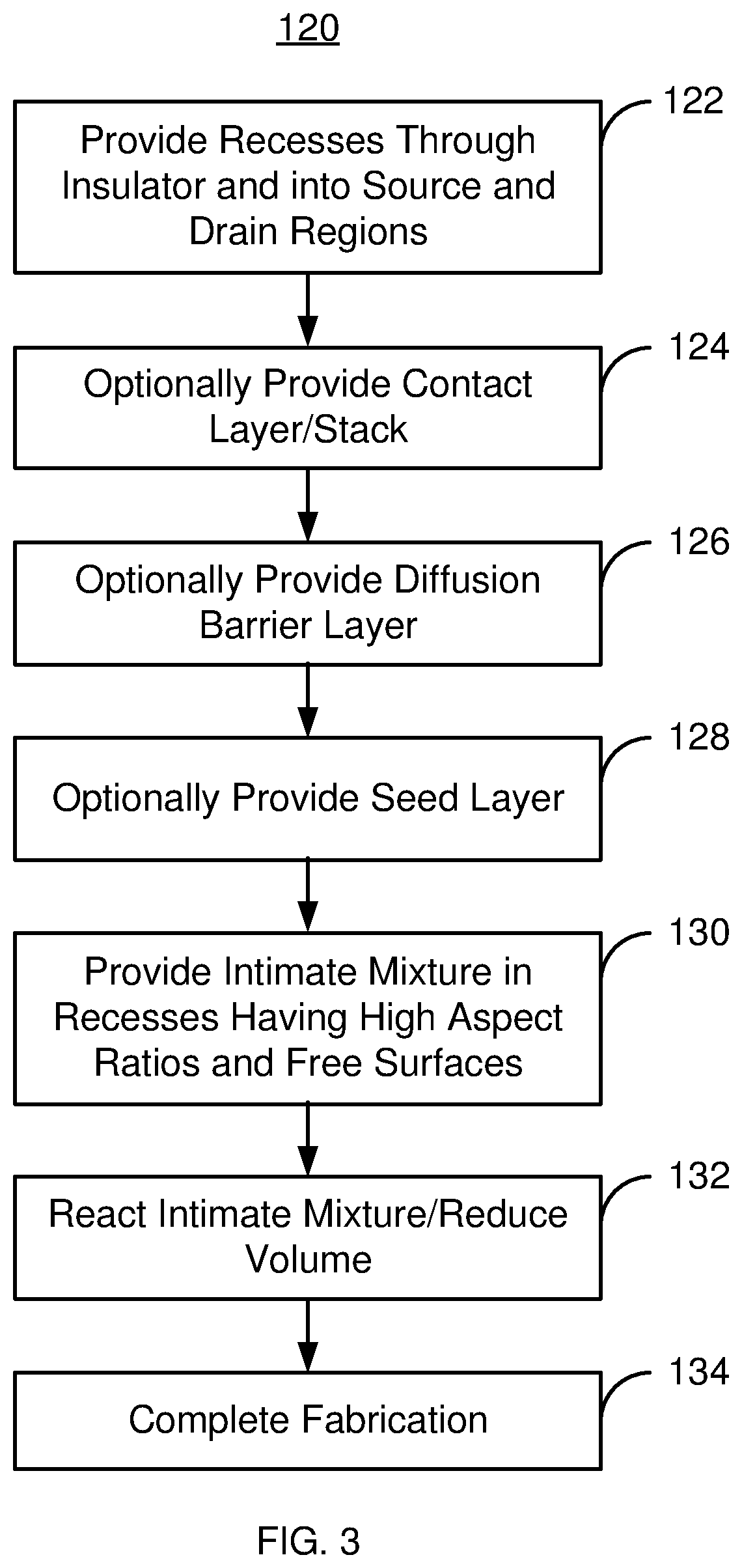
Figure 3
Abstract
Description
CROSS-REFERENCE TO RELATED APPLICATIONS
[0001] This application claims the benefit of provisional Patent Application Ser. No. 62 / 577,610, filed Oct. 26, 2017, entitled “REACTED METAL SOURCE-DRAIN STRESSOR FOR TENSILE CHANNEL STRESS”, assigned to the assignee of the present application, and incorporated herein by reference.BACKGROUND
[0002] It may be desirable to induce a strain in the channel region of a semiconductor device in order to improve performance. Strained silicon in the channel may be produced in a number of manners. For example, silicides in source and / or drain regions can induce strain in channels of metal-oxide-semiconductor MOS devices. In a MOS field effect transistor (MOSFET) a silicide in the source / drain (SD) is typically a result of the reaction of a metal layer with SD / channel materials of the MOSFET. The resulting strains induced on the channel by silicides originate from the difference in coefficients of thermal expansion between the silicide and the substrate / cha...
Examples
Embodiment Construction
[0010]The exemplary embodiments relate to formation of metal stressors for the channels of semiconductor devices such as MOS devices. The following description is presented to enable one of ordinary skill in the art to make and use the invention and is provided in the context of a patent application and its requirements. Various modifications to the exemplary embodiments and the generic principles and features described herein will be readily apparent. The exemplary embodiments are mainly described in terms of particular methods and systems provided in particular implementations. However, the methods and systems will operate effectively in other implementations.
[0011]Phrases such as “exemplary embodiment”, “one embodiment” and “another embodiment” may refer to the same or different embodiments as well as to multiple embodiments. The embodiments will be described with respect to systems and / or devices having certain components. However, the systems and / or devices may include more or ...