
Nanoporous semiconductor thin films
a semiconductor and thin film technology, applied in the field of nanoporous semiconductor thin films, can solve the problems of low sensing performance of ofet-based chemical sensors, low sensitivity, and low precision, and achieve the effects of improving sensitivity, excellent performance, and improving sensitivity
Patent Information
- Authority / Receiving Office
- US · United States
- Patent Type
- Patents(United States)
- Current Assignee / Owner
- Publication Date
- 2020-11-24
Smart Images
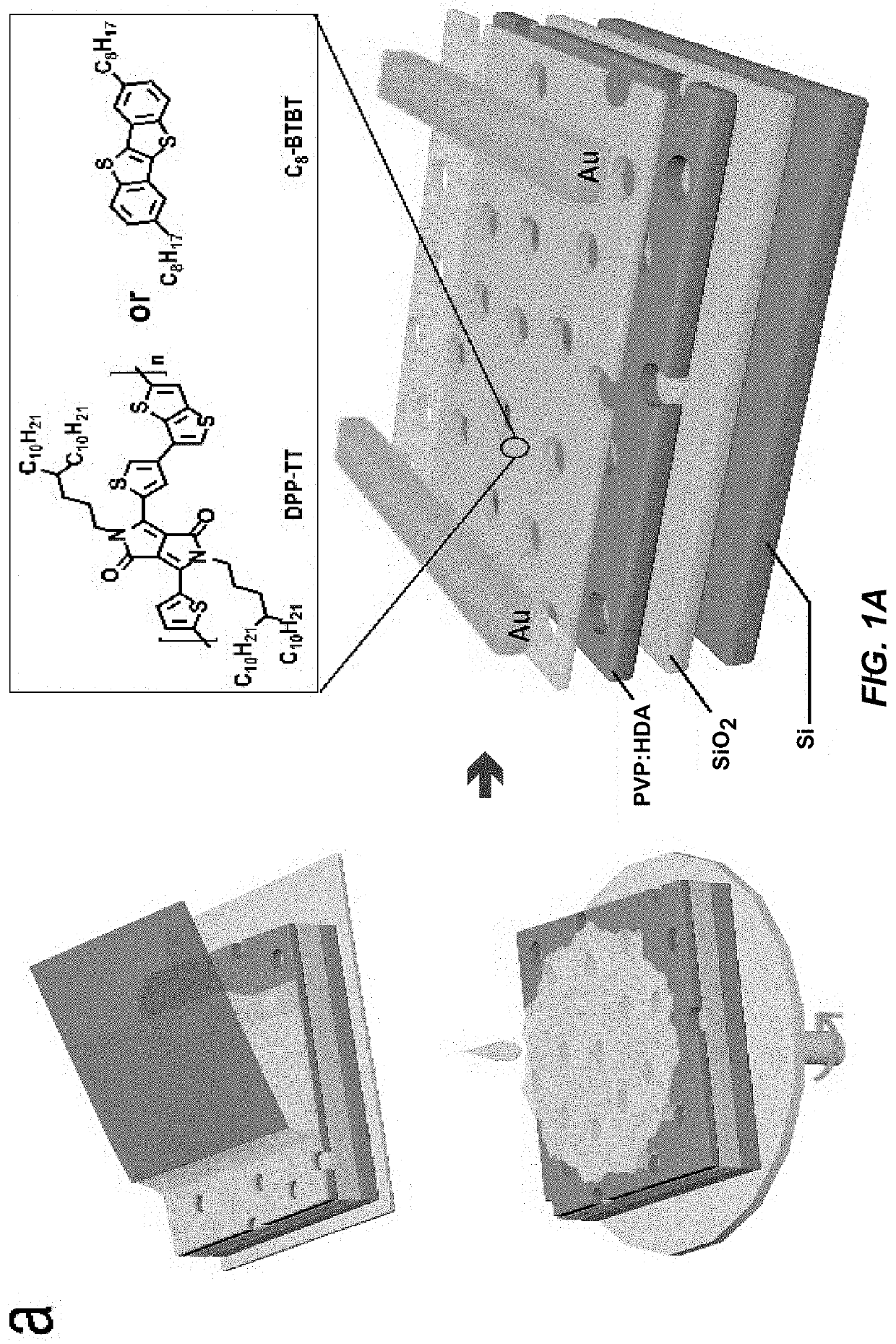
Figure 1 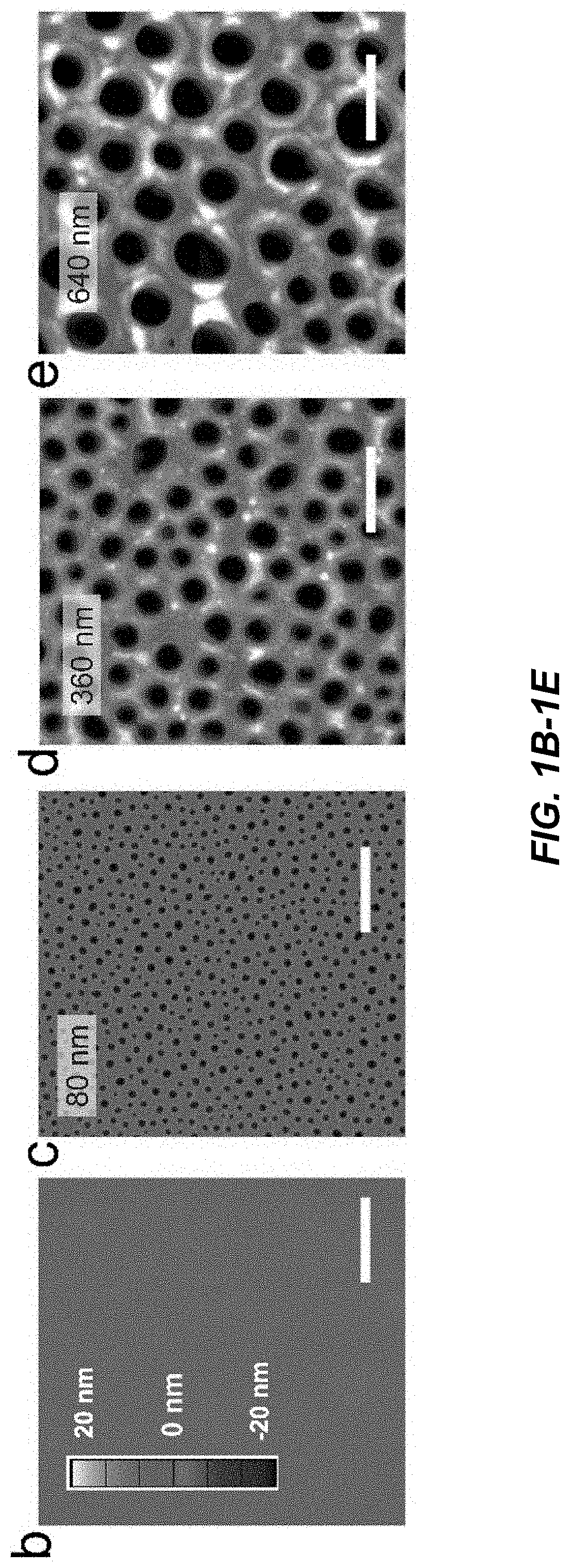
Figure 2 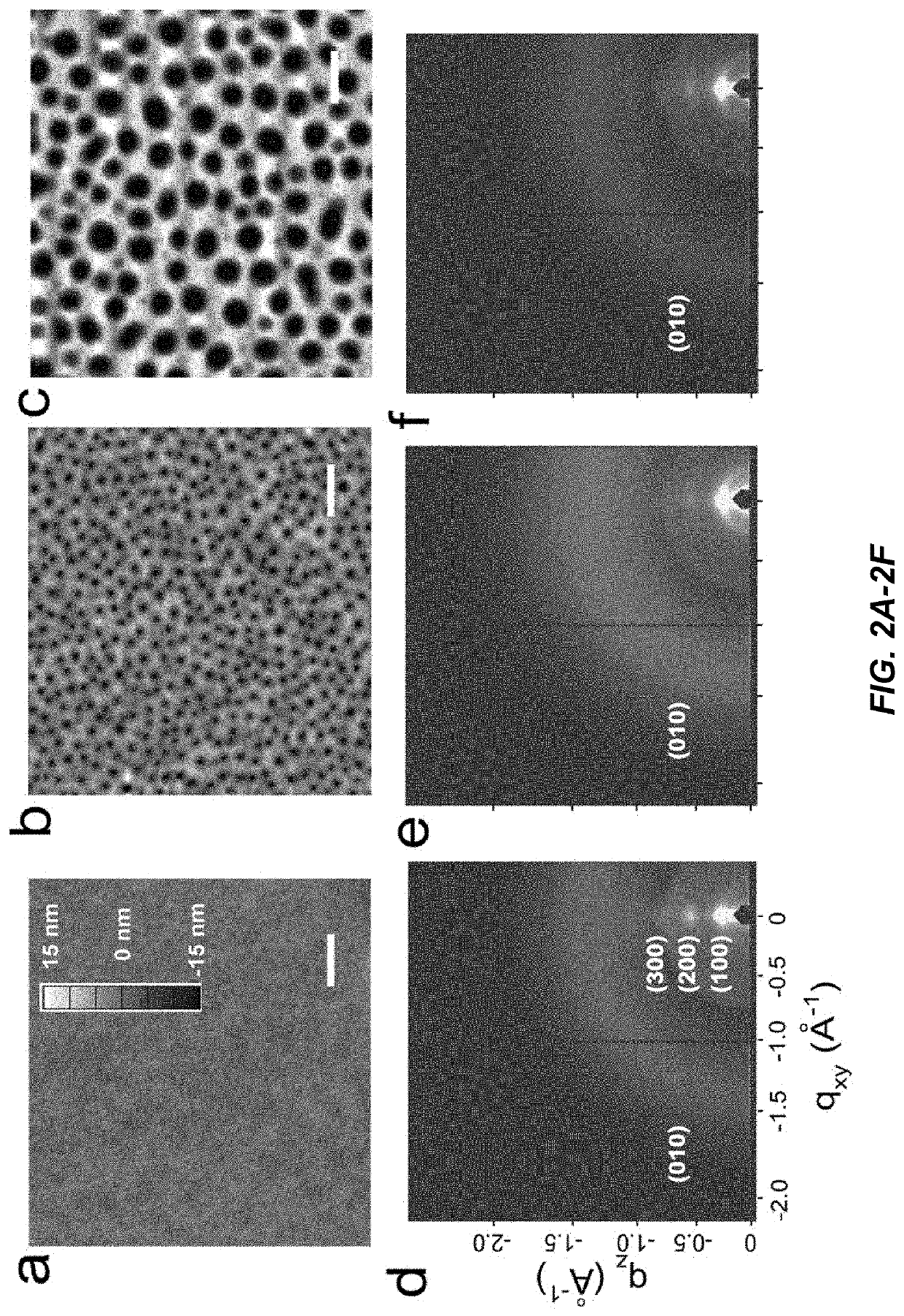
Figure 3
Abstract
Description
RELATED APPLICATIONS
[0001] This application claims priority under 35 U.S.C. § 119(e) to U.S. Provisional Patent Application No. 62 / 375,475, filed Aug. 16, 2016, which is incorporated herein by reference.BACKGROUND OF THE INVENTION
[0002] Organic semiconductors (OSC) have emerged as a new class of electronic materials promising a wide range of applications from organic field-effect transistors (OFET), solar cells, thermoelectrics, electronic skins, chemical and mechanical sensors by virtue of their chemical versatility, solution processability and mechanical flexibility. OFET-based chemical sensing presents a combination of advantages including field-effect enabled signal amplification, tunable selectivity and sensitivity by accessing vast chemical and morphological design spaces, as well as solution printability for manufacturing massively deployable low-cost sensor chips which are expected to power the Internet of Things in a foreseeable future.
[0003] Reported sensing performances of O...
Examples
example 1
g Nanoporous OSC Thin Films
[0152]We demonstrate a simple, additive approach to fabricate nanoporous semiconductor thin films in solution processing. The solution processing methods we used include spin coating and meniscus-guided unidirectional coating; the latter shares the same fundamental physics as large-scale roll-to-roll printing (FIG. 1a). The simplicity and generality of this approach for fabricating nanoporous thin films stand in contrast to the conventional subtractive approaches based on lithography and etching, which involve complex procedures and corrosive chemicals.
[0153]The key to our method is to direct the semiconductor deposition using a nanoporous insulating layer serving as the template, which can be fabricated over a large area via one-step microphase separation during spin coating. The nanoporous template was prepared from poly(4-vinylphenol) (PVP) / tetrahydrofuran (THF) solution with 4,4′-(Hexafluoroisopropylidene) diphthalic anhydride (HDA) added as the cross-...
example 2
ization of Nanoporous Semiconductor Films
[0157]We further characterized the molecular packing in the nanoporous semiconductor films by Grazing-incidence X-ray diffraction (GIXD) (FIG. 2d-f, FIGS. 9 and 10). The detailed molecular packing analysis is summarized in Table 3 and Table 4. Not surprisingly, the presence of nanopores did not noticeably alter the molecular packing in the DPP-TT thin film. FIG. 2g shows the geometrically corrected orientation distribution of crystallites in coated DPP-TT films obtained from pole-figure analysis on the π-π stacking ring. The analysis unveiled a predominant edge-on orientation of the π stacks (FIG. 2h and FIG. 9g) in all cases tested regardless of the processing methods and the pore sizes. We expect this preferred orientation to promote the charge-transfer reaction with the analyte by maximizing the exposure of the π orbitals of the conjugated core at the pore wall.
[0158]How does the nanoporous template direct the semiconductor deposition proc...
example 3
s Polymer OFET for Ammonia Sensing
[0161]To characterize the charge transport properties and sensing performance of the nanoporous semiconductor thin films, we fabricated top contact bottom gate transistor devices and performed electrical measurements under ambient conditions (FIG. 3). Typical transfer curves of DPP-TT OFETs with and without pores are shown in FIG. 3a. Both devices exhibited predominant hole transport with an on / off ratio of ˜105. The DPP-TT based nanoporous OFETs had comparable mobility (0.30±0.05 cm2V−1 s−1) but slightly lower on-current compared to the nonporous devices, due to a slight decrease in capacitance when the nanostructured template layer was introduced (FIG. 14). This observation confirms that introducing nanopores did not adversely influence the device performance. Notably, the transistor devices remained stable after repeated measurements in air, which is ideal for sensing applications (FIG. 15).
[0162]We next measured the sensing performance of DPP-TT...