
Component formation via plating technology
a technology of component formation and plating, applied in the direction of fixed capacitor details, liquid/solution decomposition chemical coating, fixed capacitors, etc., can solve the problems of difficult to print termination stripes in a predetermined area with required precision, difficult to control the application of terminations, and reduced chip sizes, so as to eliminate or greatly simplify thick-film stripes, improve termination features
Patent Information
- Authority / Receiving Office
- US · United States
- Patent Type
- Applications(United States)
- Current Assignee / Owner
- Publication Date
- 2004-12-30
- Estimated Expiration
- Not applicable · inactive patent
Smart Images
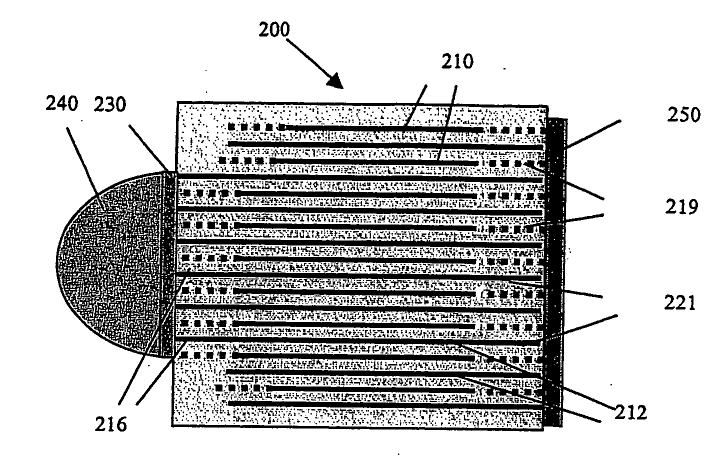
Figure 1 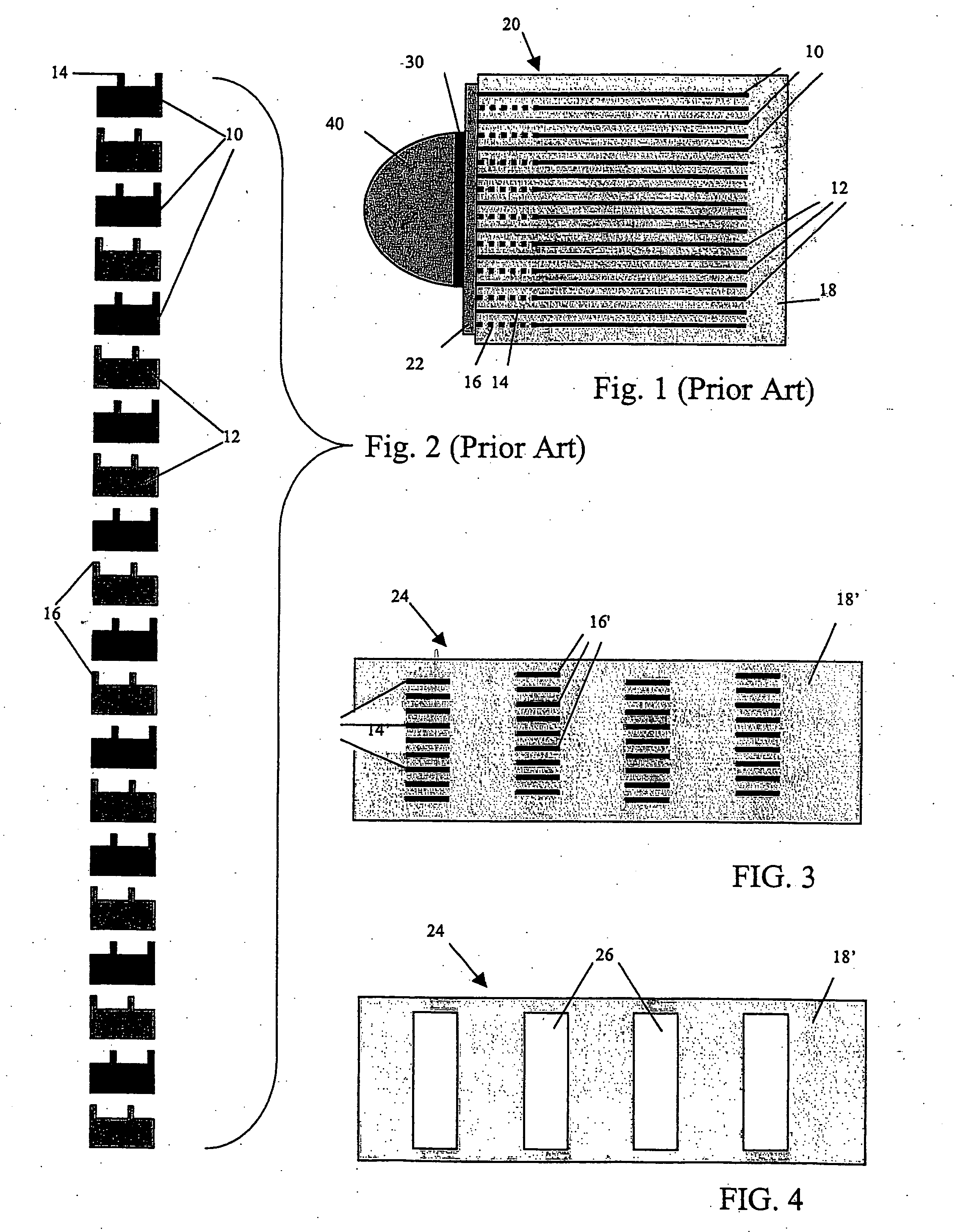
Figure 2 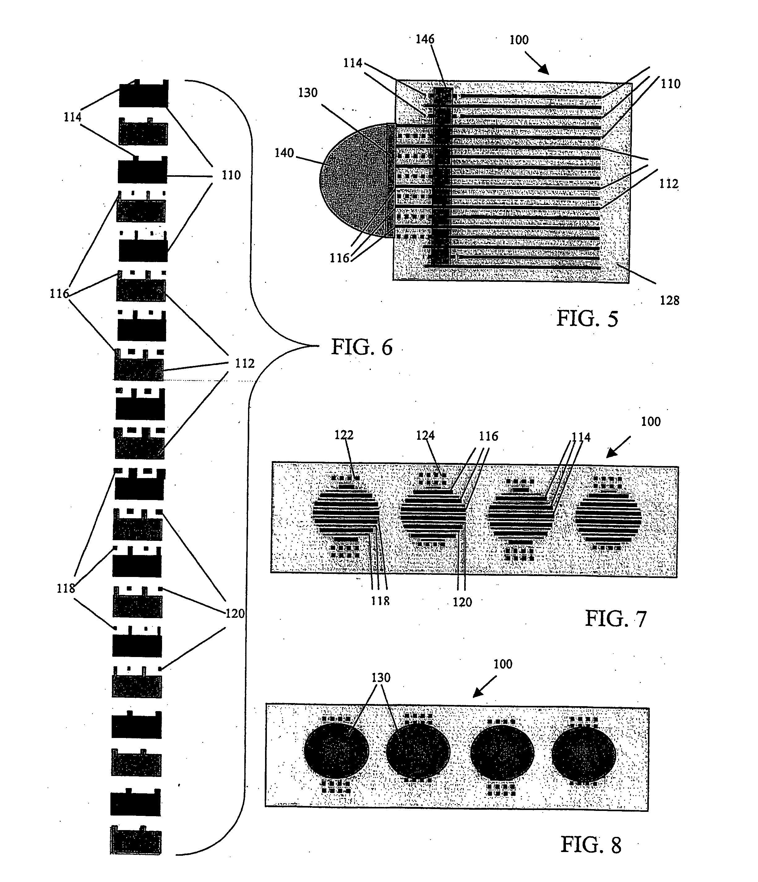
Figure 3
Abstract
Description
PRIORITY CLAIMS
[0001] This application is a continuation of U.S. patent application Ser. No. 10 / 409,036 filed Apr. 8, 2003 which, in turn, claims the benefit of U.S. Provisional Application No. 60 / 372,673, filed Apr. 15, 2002 entitled "PLATED TERMINATIONS", and U.S. Provisional Application No. 60 / 435,218, filed Dec. 19, 2002 also entitled "COMPONENT FORMATION VIA PLATING TECHNOLOGY", all of which are incorporated herein by reference for all purposes.
[0002] The present subject matter generally concerns improved component formation for multilayer electronic components. More particularly, the present subject matter relates to the utilization of plating technology in termination and inductive component formation as well as for interconnection techniques for devices such as multilayer capacitors or integrated passive components. The subject technology utilizes selective arrangements of exposed electrode tabs to facilitate the formation of plated electrical connections.
[0003] Many modern ...
Examples
embodiment 20
[0062] An interdigitated capacitor typically consists of a plurality of electrode layers, such as those shown in FIG. 2 disposed in a body of dielectric material 18, such as seen in the exemplary interdigitated capacitor (IDC) configuration 20 of FIG. 1. Electrode layers 10 and 12 are disposed in the dielectric material 18 such that electrode tabs 14 and 16 extend to and are exposed at a selected side of IDC Exemplary materials for such electrode layers may include platinum, nickel, a palladium-silver alloy, or other suitable conductive substances. Dielectric material 18 may comprise barium titanate, zinc oxide, alumina with low-fire glass, or other suitable ceramic or glass-bonded materials. Alternatively, the dielectric may be an organic compound such as an epoxy (with or without ceramic mixed in, with or without fiberglass), popular as circuit board materials, or other plastics common as dielectrics. In these cases the conductor is usually a copper foil which is chemically etche...
embodiment 24
[0073] There are several different techniques that can potentially be used to form plated terminations, such as terminations 26 on multilayer capacitor embodiment 24 of FIG. 4. As previously addressed, a first method corresponds to electroplating or electrochemical deposition, wherein an electronic component with exposed conductive portions is exposed to a plating solution such as electrolytic nickel or electrolytic tin characterized by an electrical bias. The component itself is then biased to a polarity opposite that of the plating solution, and conductive elements in the plating solution are attracted to the exposed metallization of the component. Such a plating technique with no polar biasing is referred to as electrolytic plating, and can be employed in conjunction with electroless plating solutions such as nickel or copper ionic solution.
[0074] In accordance with electrochemical deposition and electroless plating techniques, a component such as IDC 24 of FIG. 4, is preferably ...