
Logic compatible storage device
a logic and storage device technology, applied in the field of semiconductor devices, can solve the problems of specific process steps in the standard cmos-based logic process, create complications, and not only increase the wafer cost, but also fall short of the peak performance that the most advanced standard logic process can deliver. achieve the effect of improving the reliability of the memory cell, reducing leakage current for the memory array, and saving the chip area
Patent Information
- Authority / Receiving Office
- US · United States
- Current Assignee / Owner
- Publication Date
- 2008-01-10
- Estimated Expiration
- Not applicable · inactive patent
Smart Images
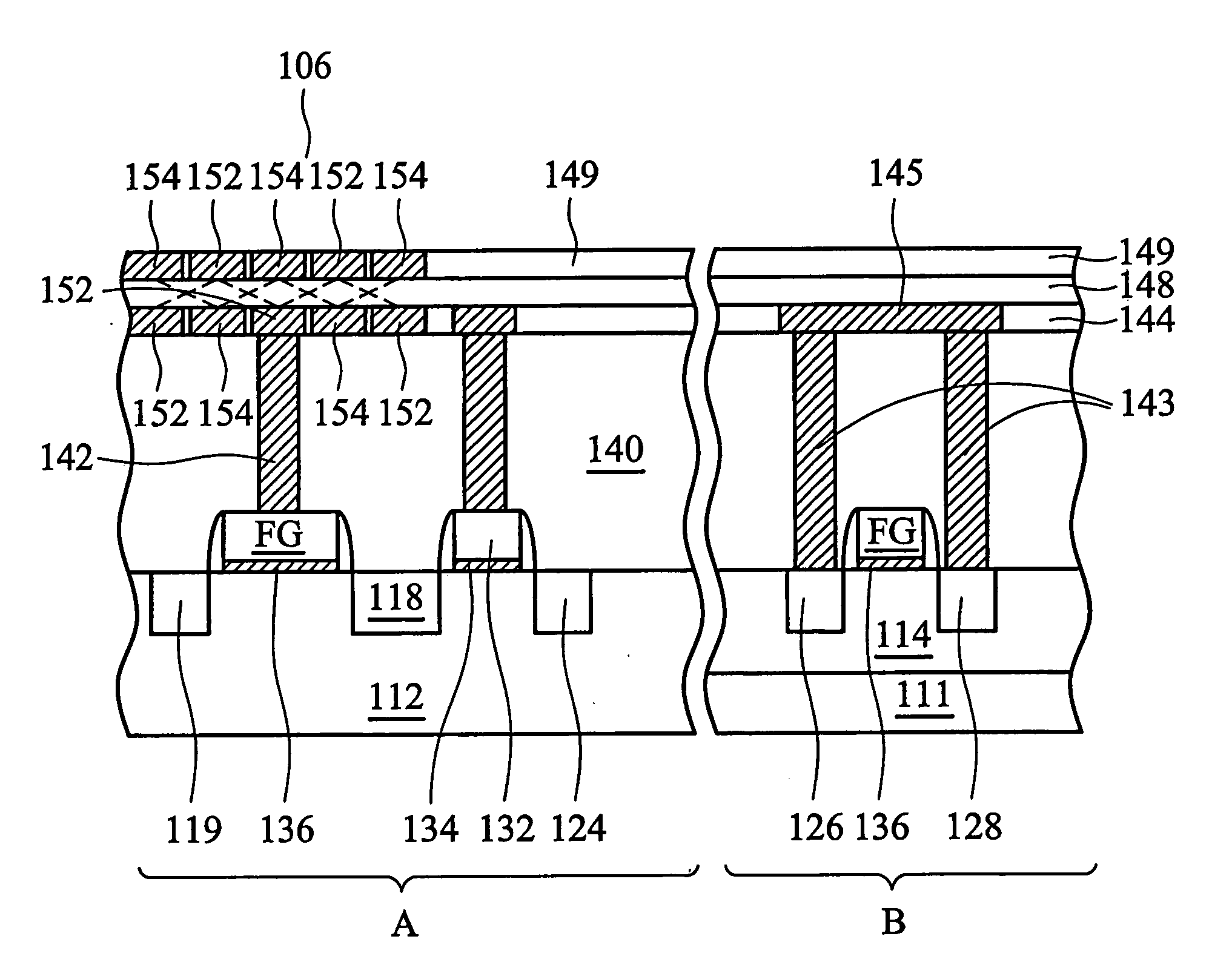
Figure 1 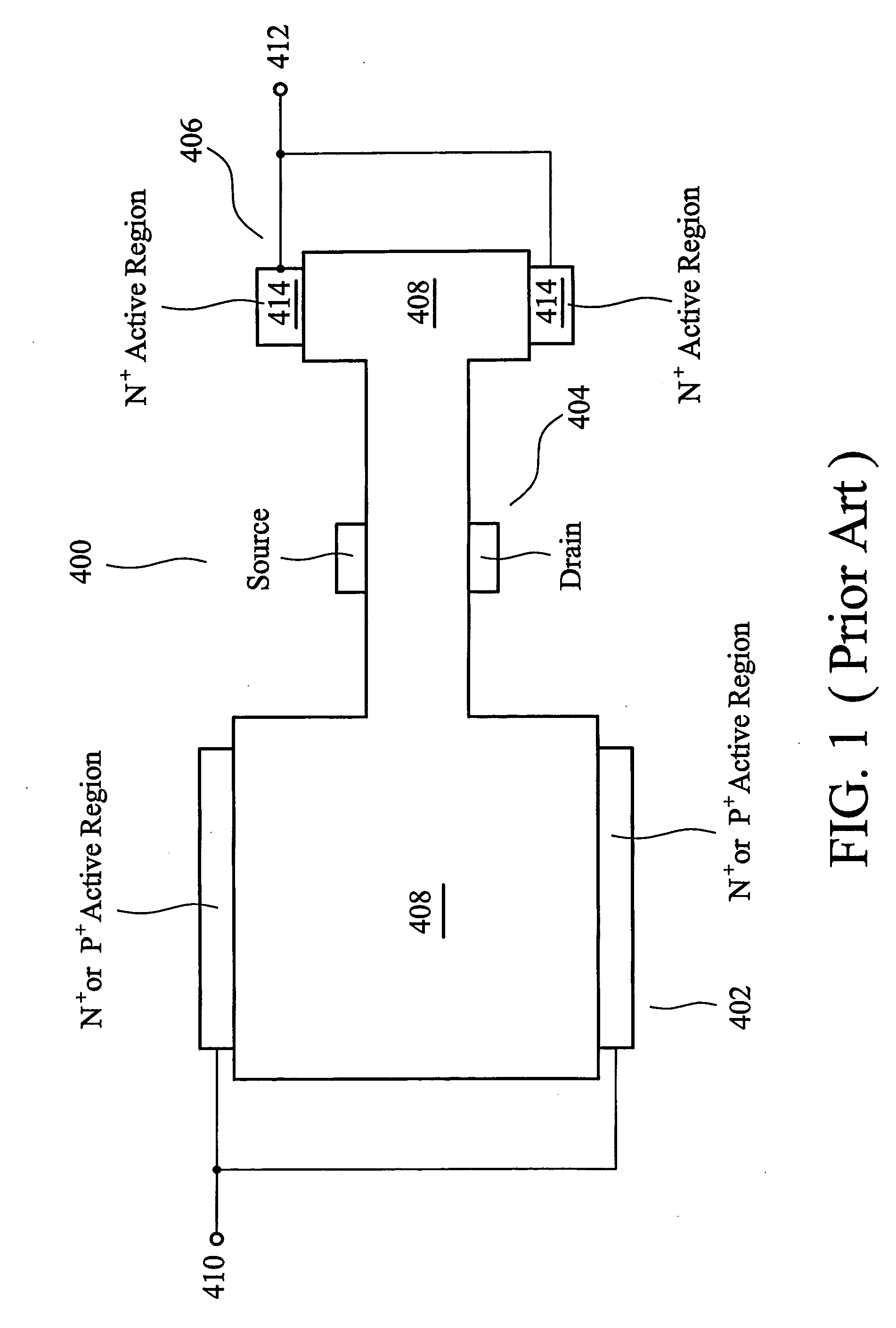
Figure 2 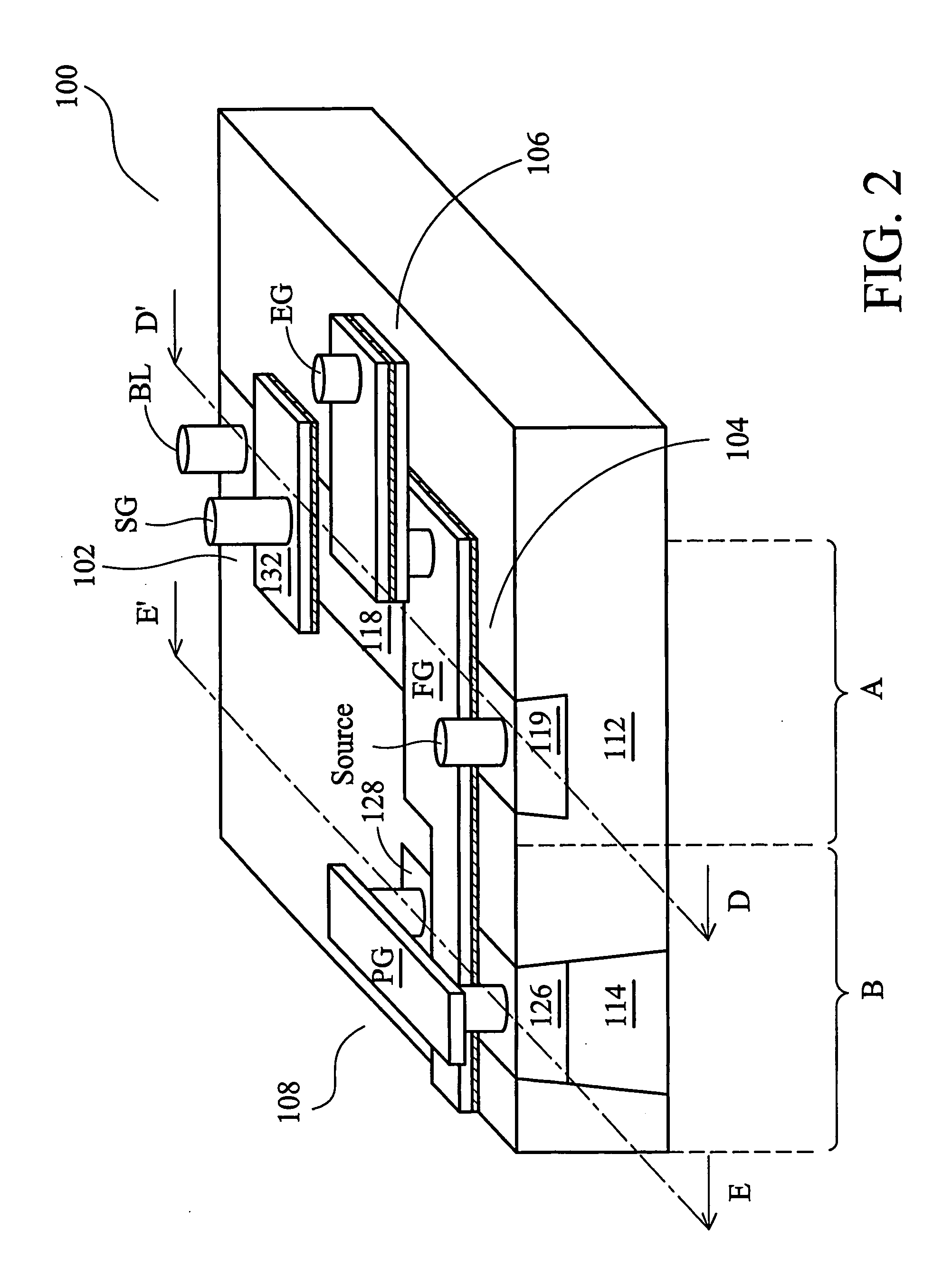
Figure 3
Abstract
Description
TECHNICAL FIELD
[0001] This invention relates generally to semiconductor devices, and more particularly to memory cells, and even more particularly to the structure and manufacturing methods of non-volatile memory cells.BACKGROUND
[0002] A non-volatile memory cell retains information stored in the memory cell even when the power is turned off. To create a non-volatile memory cell, typically a standard CMOS-based logic process is used as a starting foundation. Next, additional process steps are incorporated into the logic process flow to create the non-volatile memory cell. Examples of such additional process steps include second polysilicon deposition, junction dopant optimization, etc. Integrating “non-volatile memory”-specific process steps into the standard CMOS-based logic process creates complications. Consequently, embedded non-volatile memory technologies generally lag behind advanced logic fabrication processes by several generations. For a system-on-chip (SOC) approach, which r...
Examples
Embodiment Construction
[0018]The making and using of the presently preferred embodiments are discussed in detail below. It should be appreciated, however, that the present invention provides many applicable inventive concepts that can be embodied in a wide variety of specific contexts. The specific embodiments discussed are merely illustrative of specific ways to make and use the invention, and do not limit the scope of the invention.
[0019]A novel non-volatile memory cell and a method of forming the same are provided. The operations of the preferred embodiments are discussed. Throughout the various views and illustrative embodiments of the present invention, like reference numbers are used to designate like elements.
[0020]FIG. 2 illustrates a perspective view of a non-volatile memory cell 100, which comprises a transistor 102, a first capacitor (also referred to as an erase-tunneling capacitor) 104, a second capacitor (also referred to as a coupling capacitor) 106, and a third capacitor (also referred to ...