
Semiconductor laser chip and method of formation thereof
Patent Information
- Authority / Receiving Office
- US · United States
- Current Assignee / Owner
- Publication Date
- 2008-10-02
- Estimated Expiration
- Not applicable · inactive patent
Smart Images
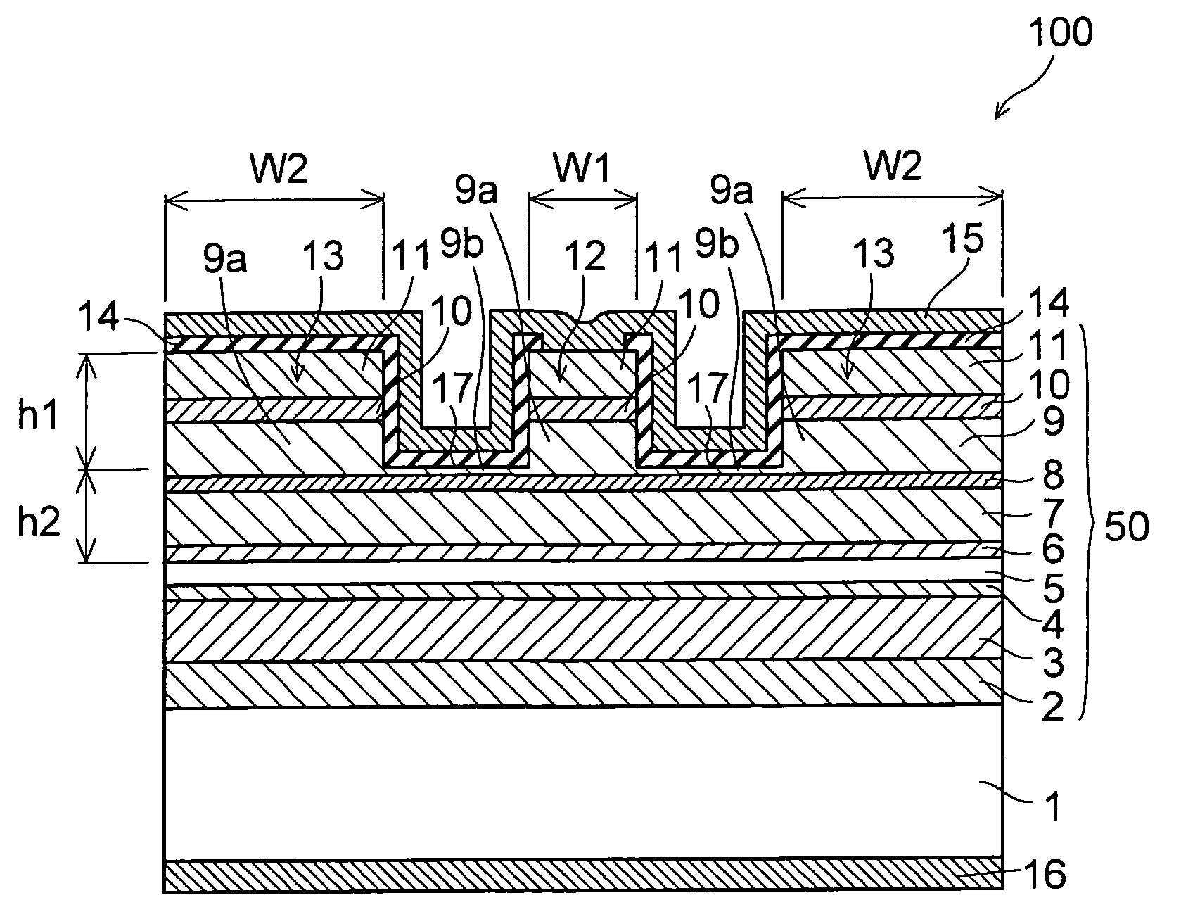
Figure 1 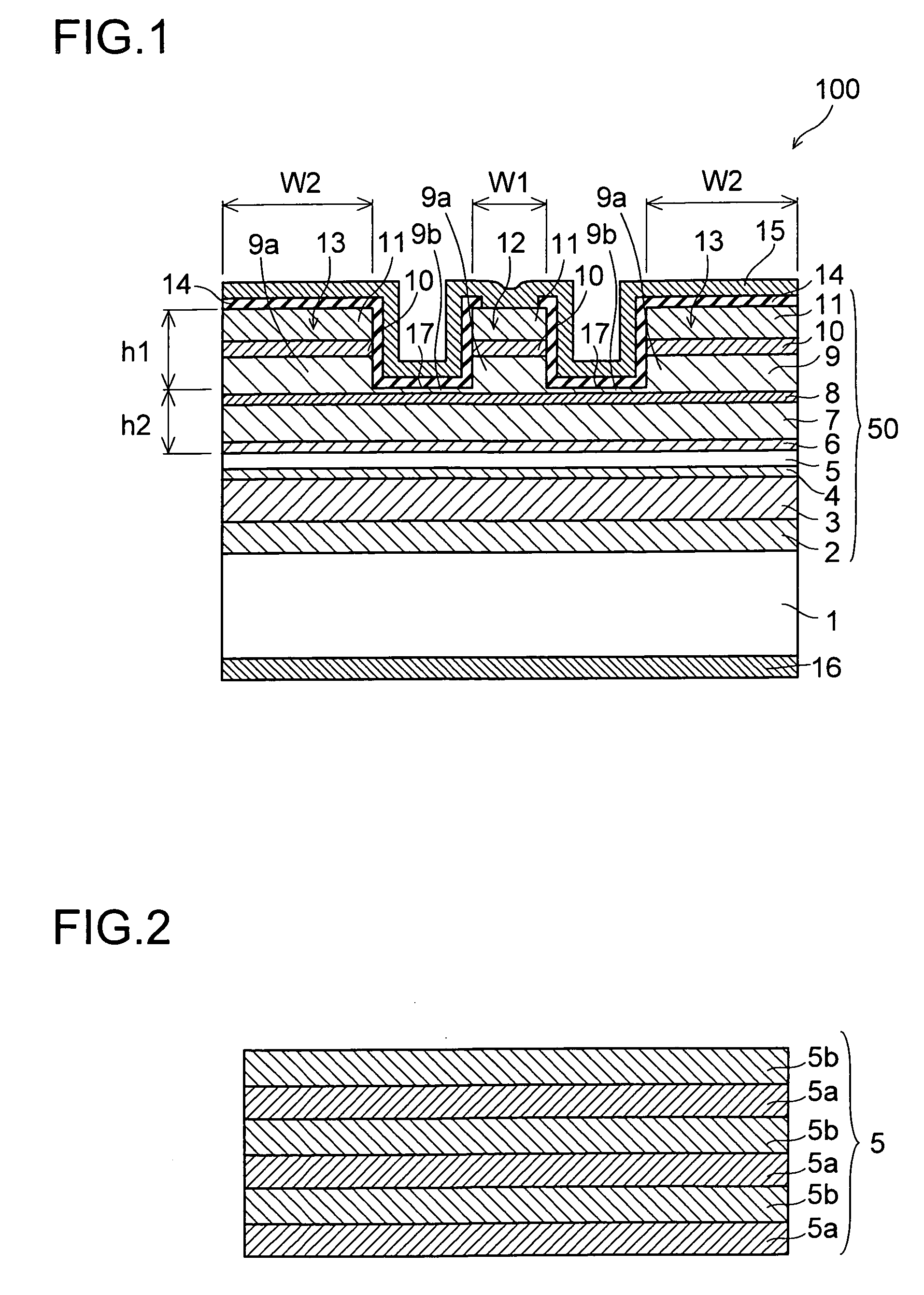
Figure 2 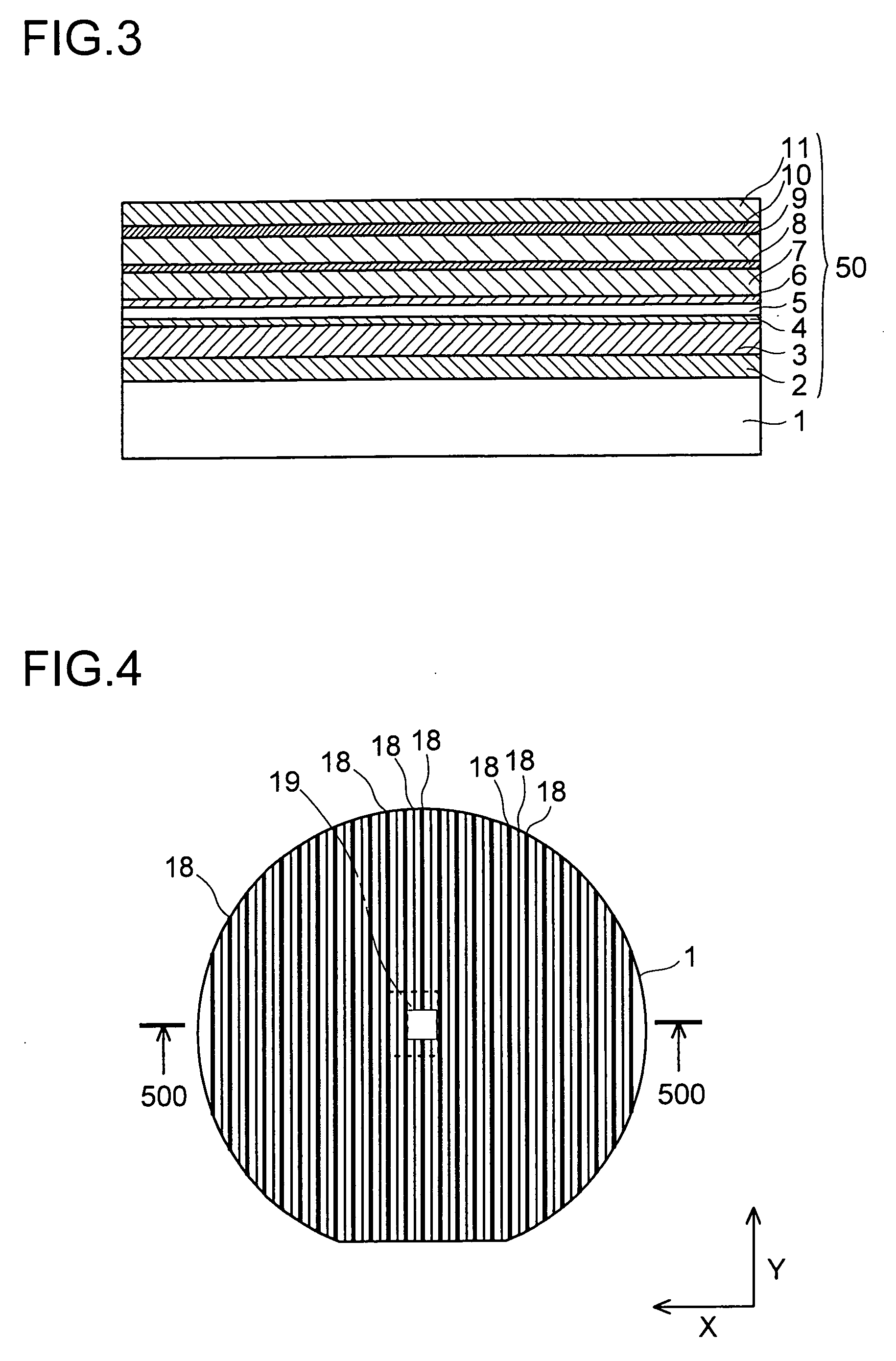
Figure 3
Abstract
Description
[0001] This nonprovisional application claims priority under 35 U.S.C. §119(a) on Patent Application No. 2007-086994 filed in Japan on Mar. 29, 2007, the entire contents of which are hereby incorporated by reference.BACKGROUND OF THE INVENTION
[0002] 1. Field of the Invention
[0003] The present invention relates to a semiconductor laser chip, and to a method of formation thereof. More specifically, the invention relates to a semiconductor laser chip provided with a ridge portion, and to a method of formation thereof.
[0004] 2. Description of Related Art
[0005] Compound semiconductor laser chips are generally provided with a stripe-shaped (long, narrow) ridge portion as a waveguide structure. The ridge portion is formed by etching a semiconductor element layer composed of a plurality of semiconductor layers laminated on a substrate.
[0006] In this case, the etching depth affects the light confinement in the horizontal-lateral direction in the light waveguide, and therefore, in etching for formi...
Examples
first embodiment
[0062]In the semiconductor laser chip 100 on an n-type GaAs substrate 1 having a thickness of about 100 μm, a layer of n-GaAs having a thickness of about 500 nm is formed as a buffer layer 2. On the buffer layer 2, a layer of n-AlxGayIn1−x−yP (where 03. On the n-type clad layer 3, a layer of undoped AlGaInP having a thickness of about 35 nm is formed as a first light guide layer 4. On the first light guide layer 4, an active layer 5 having a MQW (multiple quantum well) structure is formed. As shown in FIG. 2, the active layer 5 is composed of the following layers laminated alternately: three quantum well layers 5a, of which each is a layer of GaInP having a thickness of about 5 nm; and three barrier layers 5b, of which each is a layer of AlGaInP having a thickness of about 6 nm. It should be noted that the n-type GaAs substrate 1 is an example of a “substrate” in the invention, and that the buffer layer 2, the n-type clad layer 3, the first light guide layer 4, and the first light ...
second embodiment
[0102]In the formation process of the semiconductor laser chip 200 as described above, by forming the depressed portion 121 in the contact layer 11 by wet etching using a mixture liquid of sulfuric acid and aqueous hydrogen peroxide, it is possible to stop etching at the position where the intermediate layer 10 is exposed. That is, by the mixture liquid of sulfuric acid and aqueous hydrogen peroxide, the contact layer 111 is etched, but the intermediate layer 10 under the contact layer 111 is hardly etched. Thus, by wet etching using a mixture liquid of sulfuric acid and aqueous hydrogen peroxide, the depth of the depressed portion 121 can be adjusted to be equal to the thickness (about 85 nm) of the contact layer 111. Thus, by adjusting the thickness of the contact layer 111 to a desired thickness, even when the etching speed at the contact layer 111 varies, it is possible to adjust the depth of the depressed portion 121 accurately to a desired depth, and this helps reduce variati...
third embodiment
[0110]In the third embodiment, as described above, the ridge portion 12 is formed on the etching marker layer 8 so as to make contact therewith. This makes it possible to form the etching marker layer 8 at a desired position and thereby adjust accurately to a desired distance the distance h2 from the etching bottom surface 17 at both sides of the ridge portion 12 to an active layer 5. Thus, it is possible to easily suppress variations in the light confinement effect in the horizontal-lateral direction at both sides of the ridge portion 12. In this way, it is possible to suppress layer discontinuity in the current block layer 14 and the p-side electrode 15 and simultaneously easily reduce fabrication variations in the light radiation angle in the horizontal direction.
[0111]In other respects, the effects of the third embodiment are similar to those of the first embodiment described previously.
[0112]FIGS. 21 to 24 are sectional views illustrating the formation process of the semiconduc...