
Semiconductor device
a technology of semiconductor devices and dielectric tubes, which is applied in the direction of solid-state devices, amplifiers with semiconductor devices/discharge tubes, and basic electric elements, etc., can solve the problems of difficult to increase the resistance values of wirings, and achieve the effect of suppressing the damage of an integrated circuit due to esd
Patent Information
- Authority / Receiving Office
- US · United States
- Patent Type
- Applications(United States)
- Current Assignee / Owner
- Publication Date
- 2009-10-22
Smart Images
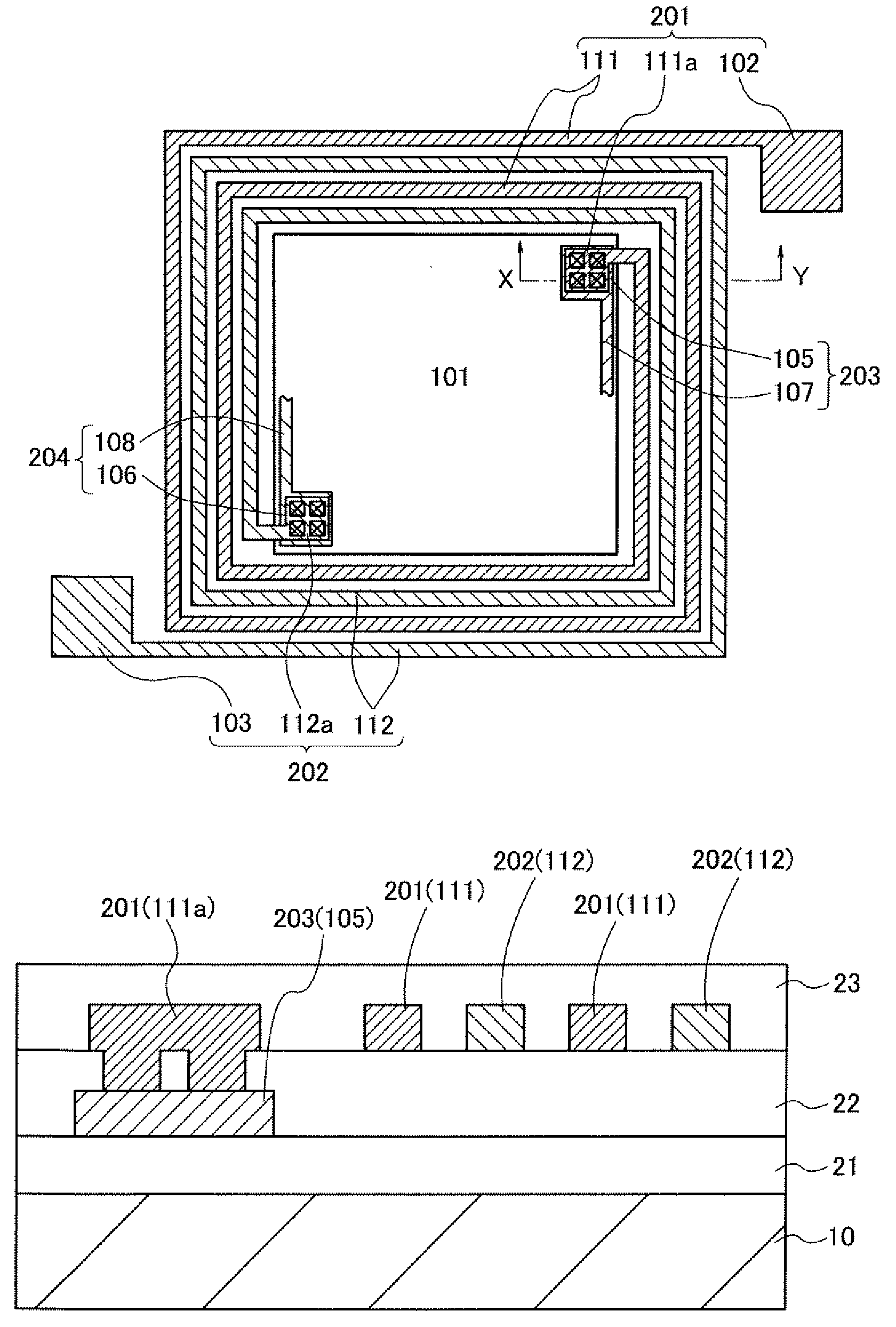
Figure 1 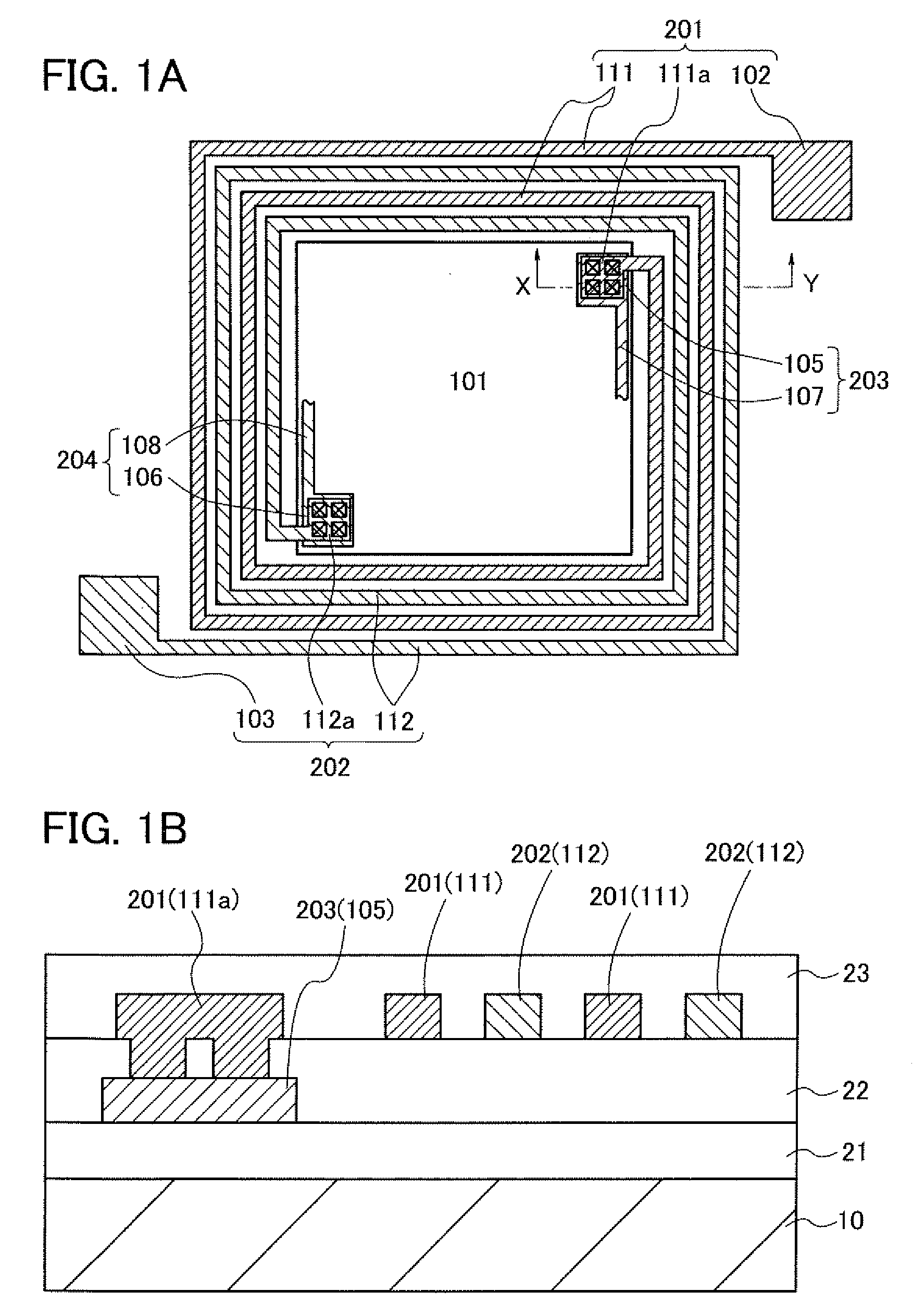
Figure 2 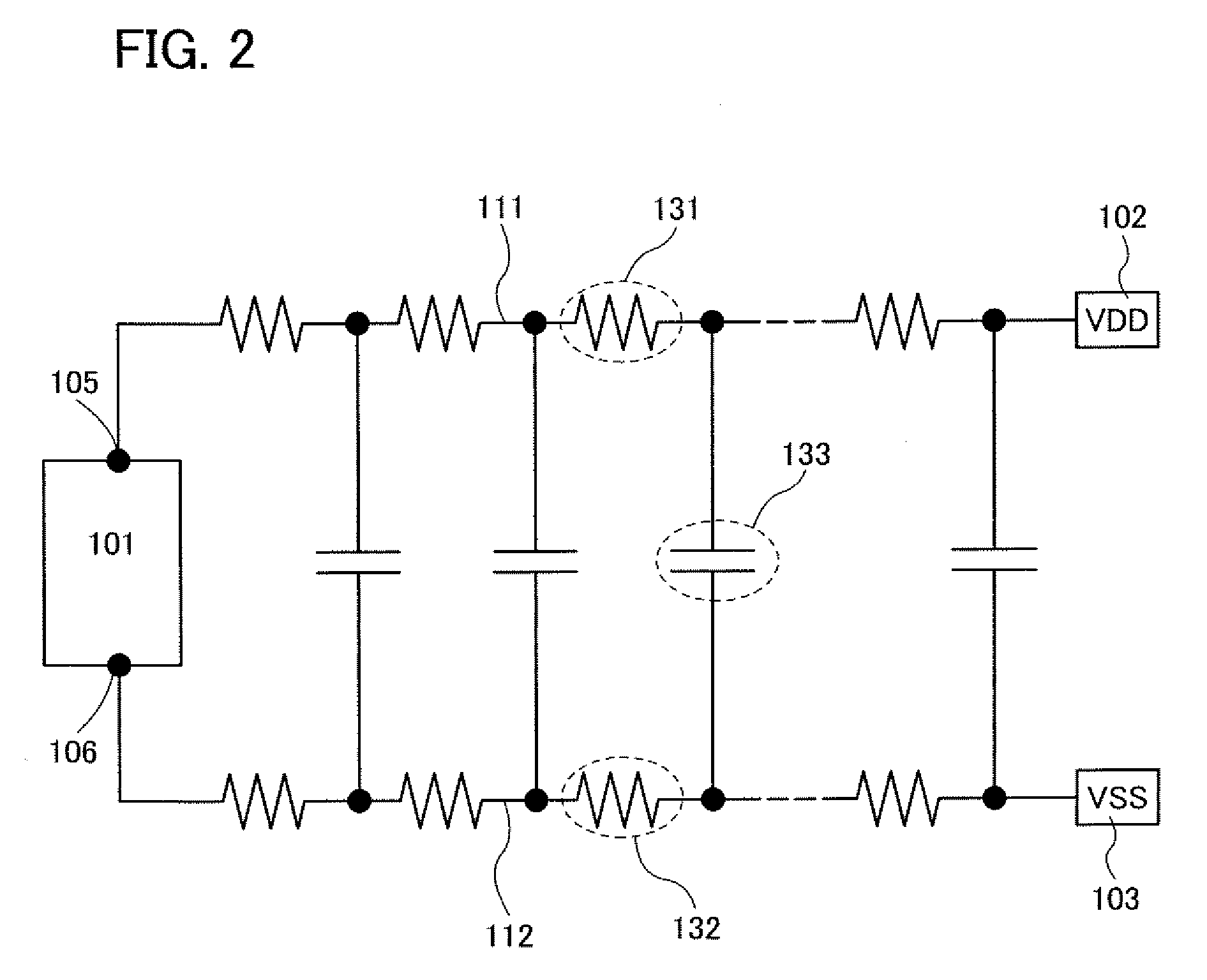
Figure 3
Abstract
Description
BACKGROUND OF THE INVENTION
[0001] 1. Field of the Invention
[0002] The present invention relates to a semiconductor device including an integrated circuit.
[0003] 2. Description of the Related Art
[0004] One of major causes of defects in integrated circuits is damage of semiconductor elements, electrodes, or the like due to electrostatic discharge (ESD). Thus, in order to prevent damage of an integrated circuit due to ESD, a protection circuit is inserted between a power supply terminal and a connection terminal for connection to an external circuit, and the integrated circuit. A protection circuit refers to a circuit for preventing the supply of overvoltage or overcurrent generated due to ESD to an integrated circuit. Typical examples of elements used for protection circuits are resistors, capacitors, diodes, and the like (see Reference 1: Japanese Published Patent Application No. 2001-339051 and Reference 2: Japanese Published Patent Application No. S63-027044).
[0005] For example, Referen...
Examples
embodiment 1
[0043]The structure of a semiconductor device of this embodiment is described with reference to FIG. 1A and FIG. 1B. FIG. 1A is a plan view illustrating the layout of the semiconductor device of this embodiment. FIG. 1B is a cross-sectional view taken along section line X-Y in FIG. 1A.
[0044]As illustrated in FIG. 1A, the semiconductor device includes an integrated circuit 101 having a plurality of semiconductor elements, a first terminal 102 to which a high power supply potential VDD is applied, a second terminal 103 to which a low power supply potential VSS is applied, a first wiring 111 which electrically connects the first terminal 102 and the integrated circuit 101 to each other, and a second wiring 112 which electrically connects the second terminal 103 and the integrated circuit 101 to each other.
[0045]The integrated circuit 101 includes a connection portion 105 electrically connected to the first wiring 111 a connection portion 106 electrically connected to the second wiring ...
embodiment 2
[0064]The structure of a semiconductor device of this embodiment is described with reference to FIG. 3A and FIG. 3B. FIG. 3A is a plan view illustrating the layout of the semiconductor device of this embodiment. FIG. 3B is a cross-sectional view taken along section line X-Y in FIG. 3A.
[0065]As illustrated in FIG. 3A, a semiconductor film 250 which overlaps with the first wiring 111 to which the power supply potential VDD is applied and the second wiring 112 to which the power supply potential VSS is applied is provided in the semiconductor device of this embodiment. The semiconductor film 250 is formed so as to surround the integrated circuit 101 in a manner similar to those of the conductive films 201 and 202. Here, the shape of the semiconductor film 250 is a quadrangle where an opening is formed in a portion overlapping with the integrated circuit 101.
[0066]As illustrated in FIG. 3B, the semiconductor film 250 is formed between the substrate 10 and the insulating film 21. The sem...
embodiment 3
[0072]In this embodiment, an example is illustrated in which each of the first wiring 111 and the second wiring 112 is formed using two conductive films which are stacked with an insulating film interposed therebetween. The structure of a semiconductor device of this embodiment is described with reference to FIG. 5A, FIG. 5B, FIG. 6A, and FIG. 6B. FIG. 5A is a plan view illustrating the layout of the semiconductor device of this embodiment. FIG. 5B is a cross-sectional view taken along section line X-Y in FIG. 5A. In addition, FIG. 6A and FIG. 6B are plan views each illustrating the layout of conductive films used for the first wiring 111 and the second wiring 112. FIG. 6A is a plan view of a second conductive film. FIG. 6B is a plan view of a first conductive film.
[0073]As illustrated in FIG. 5A, the first wiring 111 includes the conductive film 201 and the conductive film 203 which is used for the connection portion 105. In addition, the second wiring 112 includes the conductive f...