
Semiconductor device and method of manufacturing semiconductor device including wiring via and switch via for connecting first and second wirings
a semiconductor device and semiconductor technology, applied in semiconductor devices, semiconductor/solid-state device details, electrical equipment, etc., can solve the problems of loss of information on the configured function, increase in the price of a semiconductor chip, and increase in the cost of a photolithography mask used in forming a circuit pattern necessary for performing a desired function, etc., to suppress damage to the surface of the wiring or the resistance change layer.
Patent Information
- Authority / Receiving Office
- US · United States
- Patent Type
- Patents(United States)
- Current Assignee / Owner
- Publication Date
- 2013-03-05
- Estimated Expiration
- Not applicable · inactive patent
Smart Images
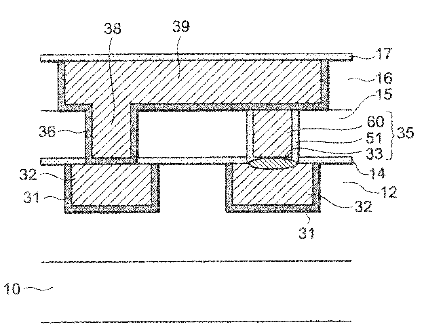
Figure 1 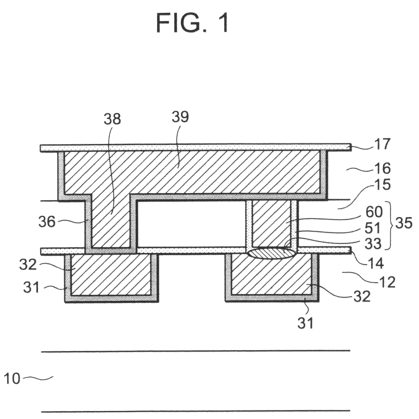
Figure 2 
Figure 3
Abstract
Description
BACKGROUND OF THE INVENTION
[0001] 1. Field of the Invention
[0002] The present invention relates to a semiconductor device and a method of manufacturing a semiconductor device.
[0003] 2. Description of the Related Art
[0004] As more and more precise technologies are necessary for manufacturing a semiconductor device, the cost of a mask for photolithography used in forming a circuit pattern necessary for performing a desired function increases, and, as a result, the price of a semiconductor chip increases. In order to avoid such a problem of the cost of the mask, a semiconductor chip referred to as a field programmable gate array (FPGA) having a function which is programmable according to the purpose of the chip is sometimes used. The FPGA may perform various functions by changing its circuit configuration with a switch. Typically used as the switch is a static random access memory (SRAM) device including a plurality of transistors. In such device, information on the configured function is ...
Examples
first embodiment
[0039]FIG. 1 is a sectional view illustrating a configuration of a semiconductor device according to a first embodiment. The semiconductor device includes a substrate 10, a first wiring layer 12, a second wiring layer 16, and a switch via 35. The substrate 10 is a semiconductor substrate made of, for example, silicon, and has an active element such as a transistor formed thereon. The first wiring layer 12 is formed on the substrate 10. The first wiring layer 12 includes first wiring 32 while the second wiring layer 16 includes second wiring 39. The switch via 35 connects the first wiring 32 and the second wiring 39. Further, the switch via 35 includes at least at its bottom a switch element which has a resistance change layer 33. The resistance value of the resistance change layer 33 changes according to the history of the applied electric field. The resistance change layer 33 is, for example, a metal oxide layer such as an oxide layer of copper. The resistance change layer 33 is no...
second embodiment
[0059]FIG. 5 is a sectional view illustrating a configuration of a semiconductor device according to a second embodiment. The semiconductor device has a configuration similar to that of the semiconductor device according to the first embodiment except for the following points. First, the switch element includes a lower electrode layer 41. Secondly, the resistance change layer 33 is formed on top of the lower electrode layer 41. Thirdly, the upper electrode layer 51 is not formed and the metal layer 60 functions as an upper electrode.
[0060]The lower electrode layer 41 is located between the first wiring 32 and the resistance change layer 33. The lower electrode layer 41 and the resistance change layer 33 are formed at the bottom and on the side of the switch via 35.
[0061]Next, a method of manufacturing the semiconductor device illustrated in FIG. 5 is described with reference to FIG. 6. The method of manufacturing the semiconductor device is similar to that of the case of the first e...
third embodiment
[0067]FIG. 7 is a sectional view illustrating a configuration of a semiconductor device according to a third embodiment. The semiconductor device has a configuration similar to that of the semiconductor device according to the second embodiment except that the upper electrode layer 51 is formed between the metal layer 60 and the resistance change layer 33 of the switch via 35. More specifically, in this embodiment, the lower electrode layer 41, the resistance change layer 33, and the upper electrode layer 51 are formed at the bottom and on the side of the switch via 35.
[0068]According to this embodiment, effects similar to those of the second embodiment may be obtained.