
Method and A System for Producing a Semi-Conductor Module
a semi-conductor module and semi-conductor technology, applied in the direction of individual semiconductor device testing, semiconductor/solid-state device testing/measurement, instruments, etc., can solve the problems of insufficient quantity of desired electric contact, easy error in bumping contact, complex wiring form, etc., to achieve rapid and economical changes or adaptations, and increase the cost of modules
Patent Information
- Authority / Receiving Office
- US · United States
- Patent Type
- Applications(United States)
- Current Assignee / Owner
- Publication Date
- 2013-03-07
Smart Images
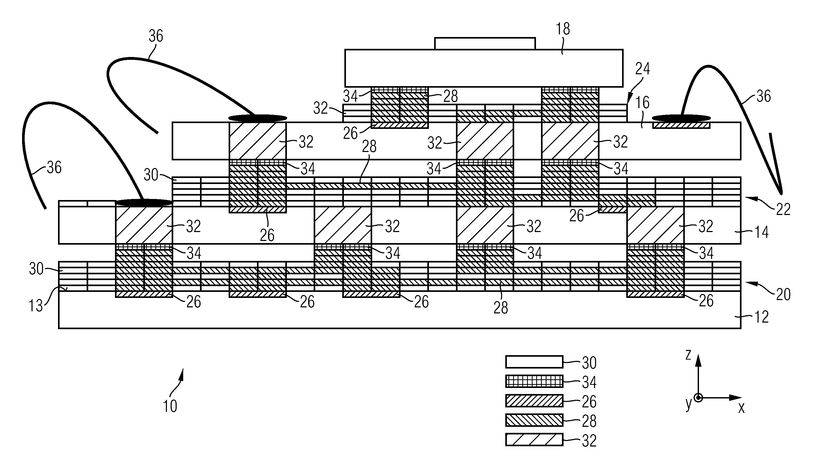
Figure 1 
Figure 2 
Figure 3
Abstract
Description
BACKGROUND TO THE INVENTION
[0001] The invention relates to a semi-conductor module and to a method and a system for producing this type of semi-conductor module.
[0002] As mobile electronics become more and more significant, conventional printed circuit boards with active or passive components, such as semi-conductor chips, applied to them two-dimensionally are becoming less significant. The electric or electronic components are stacked three-dimensionally. The aim here is to stack as many chips as possible in the form of a “stack” within the height of an individual housing. This technology is supported by very thin wafers which are being produced to be better and better. If the material thicknesses of thinned wafers—and so also of the individual silicon sheets—came within the range of over 150 μm in the past, material thicknesses of below 50 μm are currently possible.
[0003] This development also corresponds to the legality known as Moore's law according to which the electronics in semi...
Examples
Embodiment Construction
[0051]In the exemplary embodiments described below elements which are similar to one another functionally or structurally are provided as far as possible with the same or similar reference numbers. Therefore, in order to understand the features of the individual elements of a specific exemplary embodiment, reference is made to the description of other exemplary embodiments or to the general description of the invention.
[0052]In order to facilitate the description of the projection exposure tool a Cartesian xyz coordinate system is specified in the drawings from which the respective relative position of the components shown in the figures is clear. In FIG. 1 the y direction runs perpendicular to the plane of the drawing and away from the latter, the x direction to the right, and the z direction upwards.
[0053]FIG. 1 shows a diagrammatic illustration of a semi-conductor module 10 according to the invention in a sectional view. This is a three-dimensionally integrated module in which a ...