
Illumination Systems and Methods for Photoluminescence Imaging of Photovoltaic Cells and Wafers
a photovoltaic cell and photoluminescence imaging technology, applied in the field of illumination systems, can solve the problems of significant light safety issues in the prior art laser-based pl imaging system, extreme intensity of image formed on the retina, and short measurement time, so as to improve the thermal emission of the wafer or cell, the effect of shortening the measurement time and high intensity illumination
Patent Information
- Authority / Receiving Office
- US · United States
- Patent Type
- Applications(United States)
- Current Assignee / Owner
- Publication Date
- 2013-03-14
- Estimated Expiration
- Not applicable · inactive patent
Smart Images
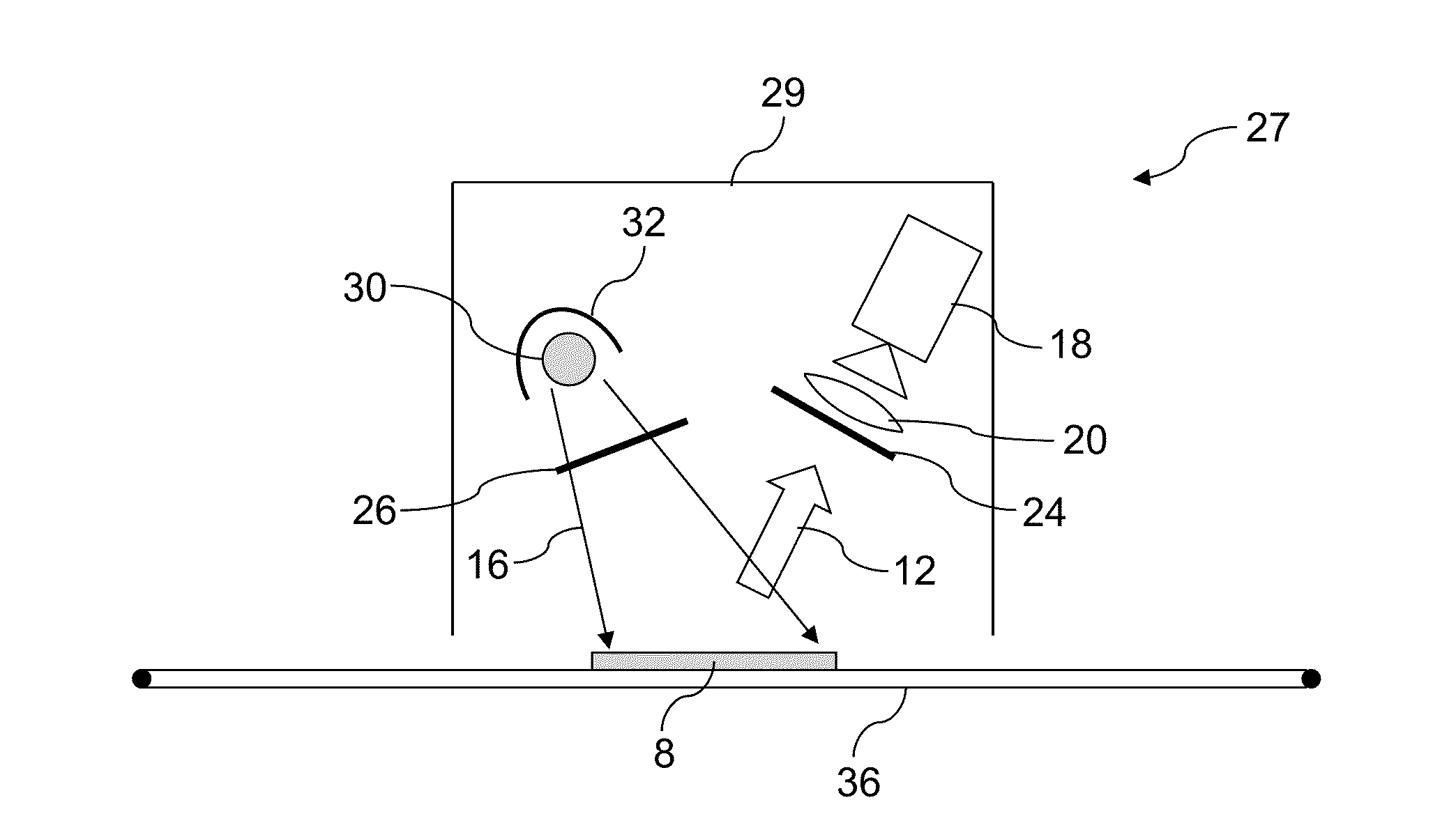
Figure 1 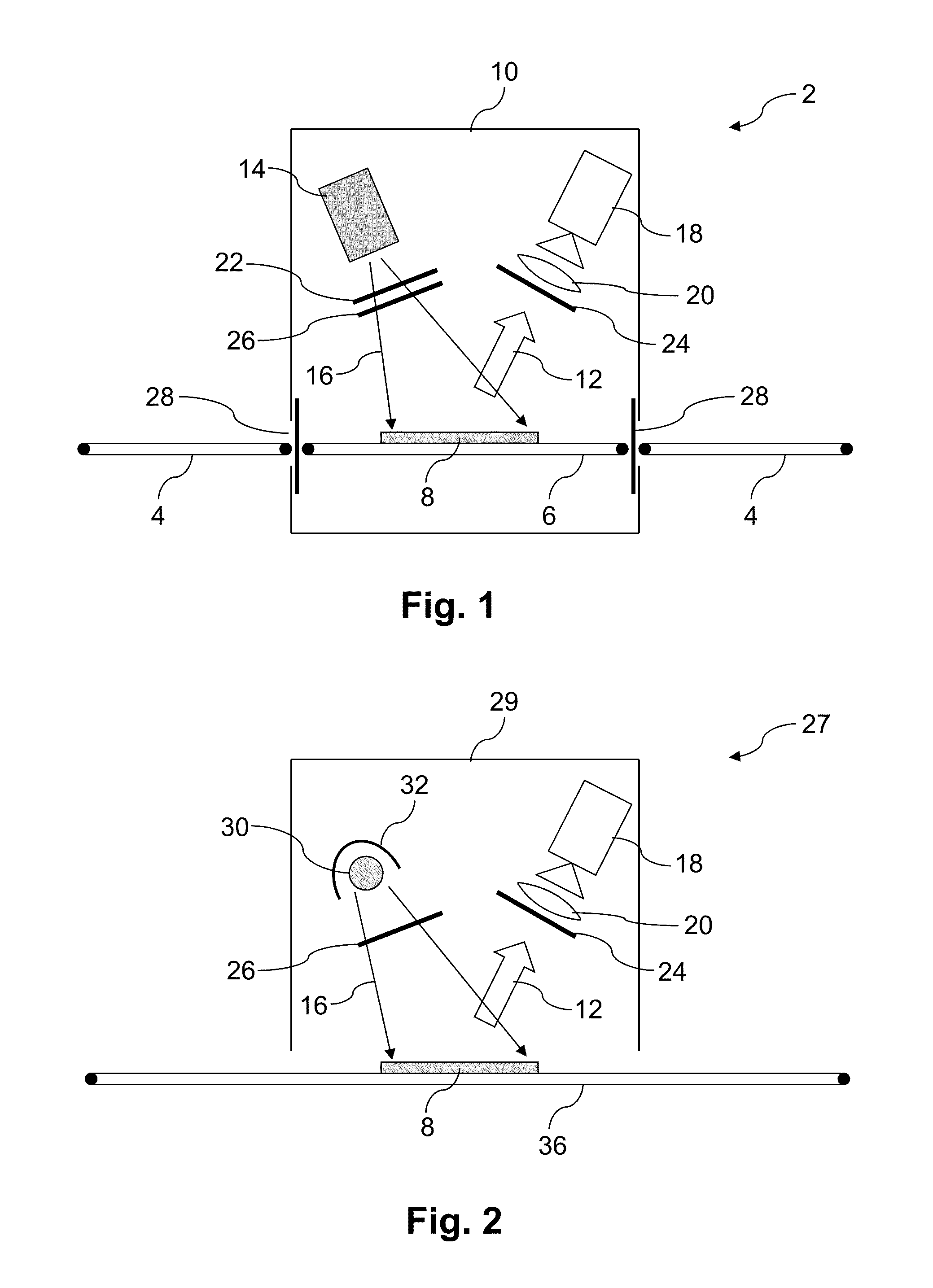
Figure 2 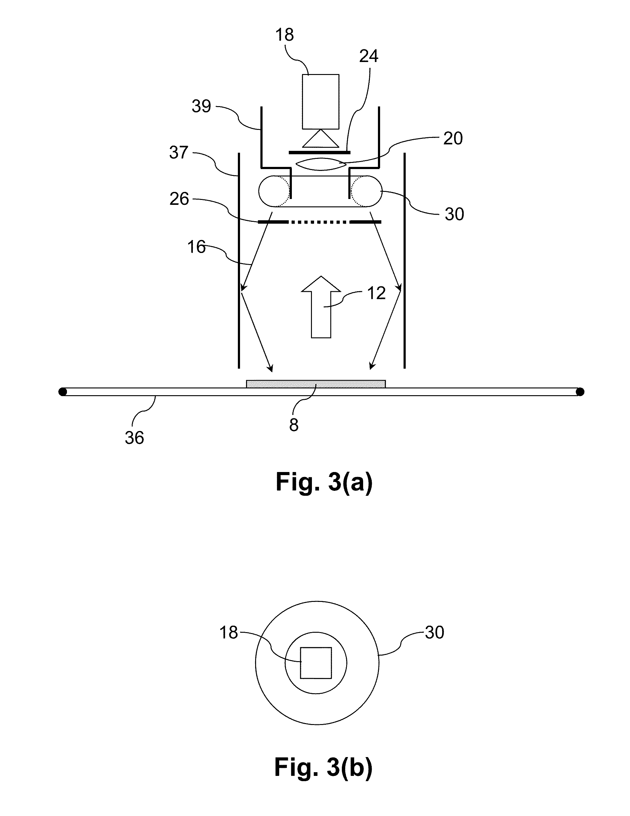
Figure 3
Abstract
Description
FIELD OF THE INVENTION
[0001] The present invention relates to illumination systems, and methods using these systems, for the characterisation of semiconductor materials using photoluminescence imaging. The illumination systems have particular application to the characterisation of silicon-based photovoltaic cells and cell precursors.RELATED APPLICATIONS
[0002] The present application claims priority from Australian provisional patent application Nos 2010900018, 2010903050 and 2010903975, the contents of which are incorporated herein by reference.BACKGROUND OF THE INVENTION
[0003] Any discussion of the prior art throughout this specification should in no way be considered as an admission that such prior art is widely known or forms part of the common general knowledge in the field.
[0004] The semiconductor industry has for decades used photoluminescence (PL), the generation of luminescence with above band gap excitation, as a non-destructive method for investigating direct band gap semicond...
Examples
Embodiment Construction
[0058]Preferred embodiments of the invention will now be described, by way of example only, with reference to the accompanying drawings.
[0059]Photoluminescence (PL) imaging is known to be a rapid and convenient technique for characterising silicon ingots, blocks, wafers, as well as silicon-based photovoltaic (PV) cells both during and after manufacture, using systems and methods described in the abovementioned published PCT patent application No WO 07 / 041,758 A1. The PL emission from silicon arises primarily from band-to-band recombination in the wavelength range 900 to 1300 nm, and can provide information on many material, mechanical and electrical parameters of relevance to PV cell performance including minority carrier diffusion length and minority carrier lifetime, and the impact of certain materials impurities and defects on the these properties.
[0060]FIG. 1 shows a PL imaging system 2 suitable for acquiring PL images of semiconductor devices such as silicon PV cells during the...