
Ltps array substrate
Patent Information
- Authority / Receiving Office
- US · United States
- Current Assignee / Owner
- Publication Date
- 2016-11-24
Smart Images
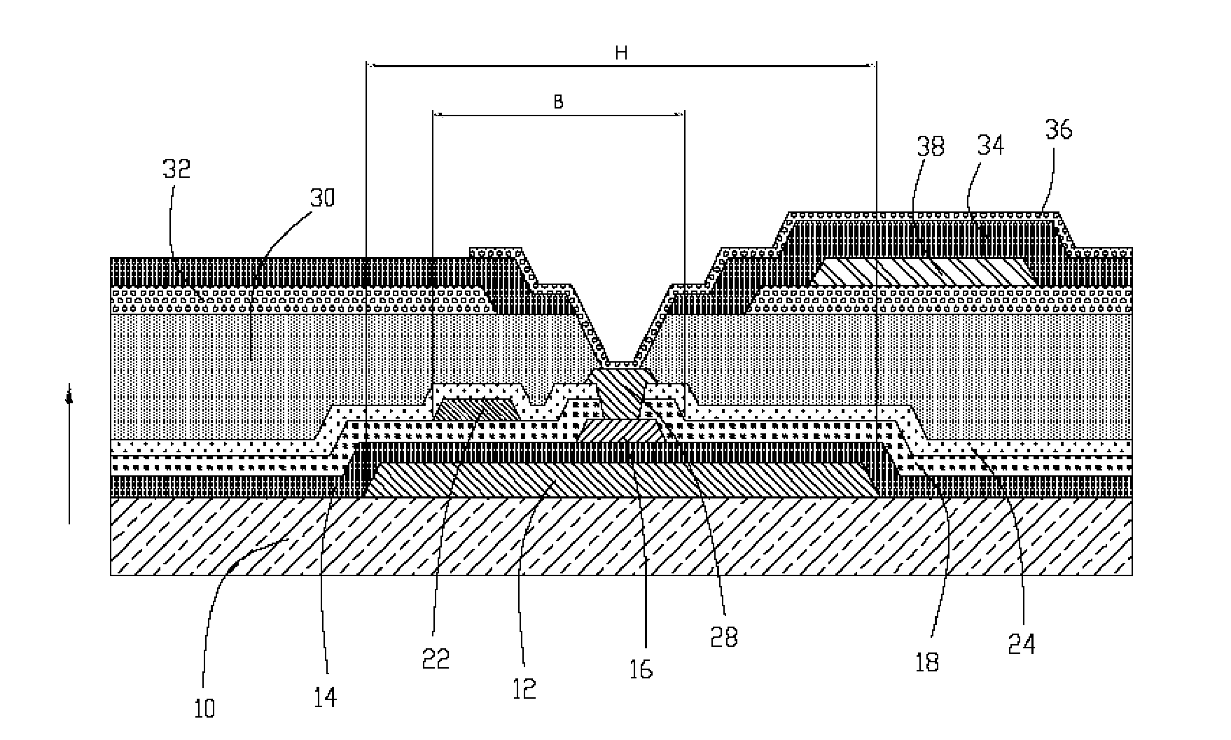
Figure 1 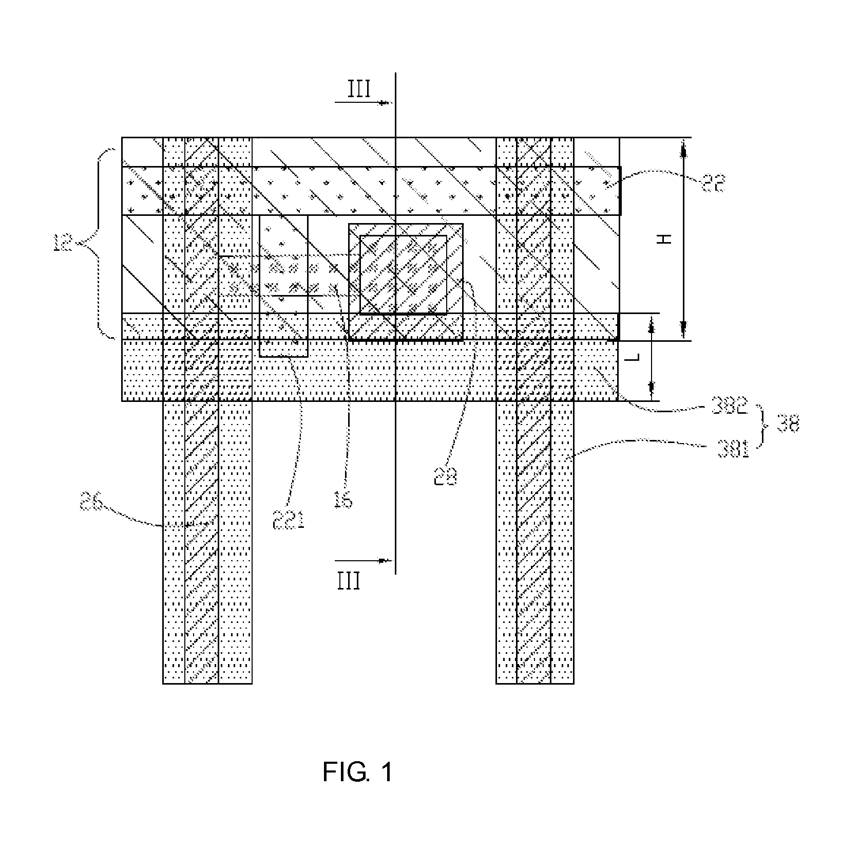
Figure 2 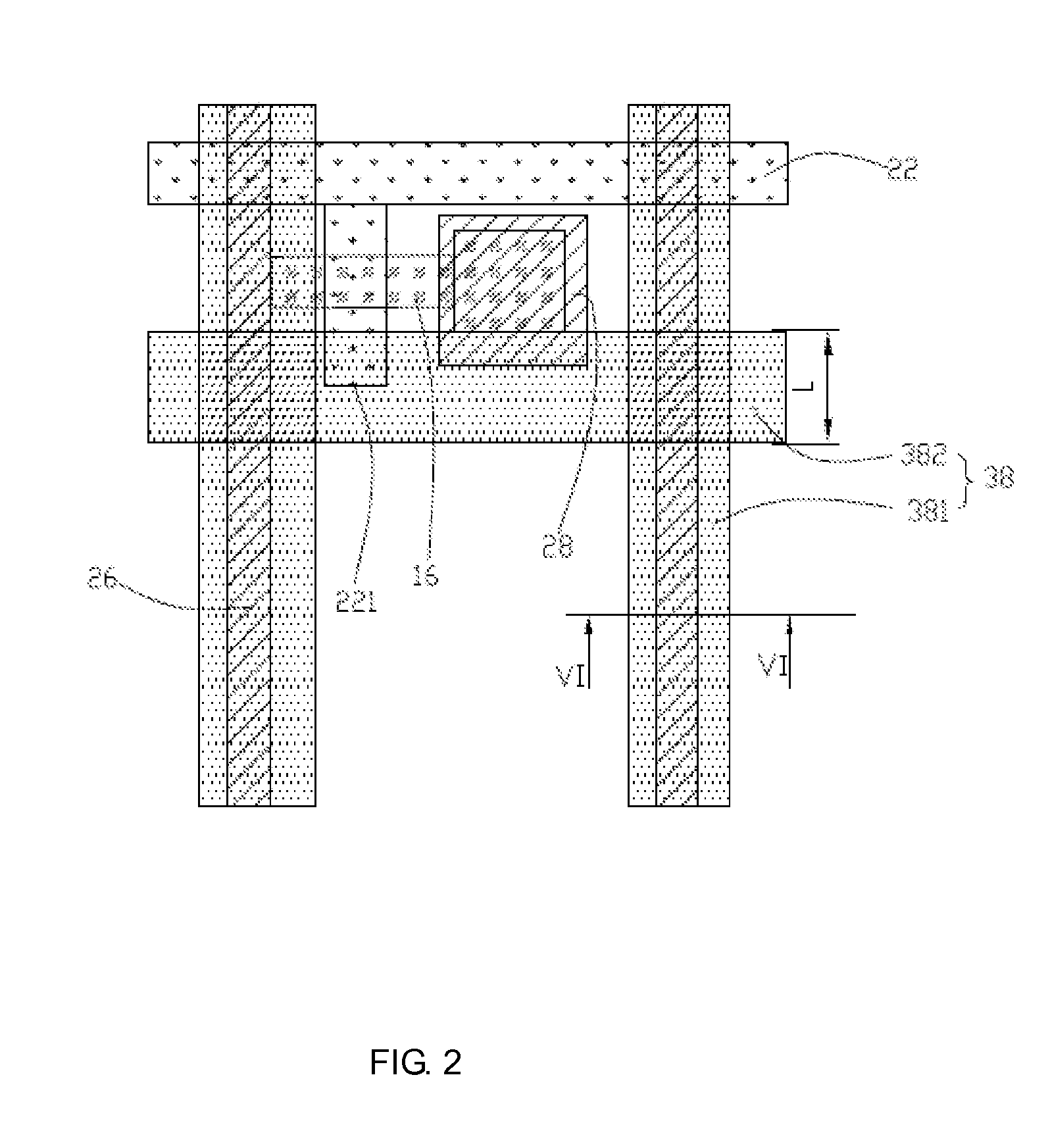
Figure 3
Abstract
Description
CROSS REFERENCE TO RELATED APPLICATIONS
[0001] This application claims the priority of Chinese Patent Application No. 201410784820.4, entitled “LTPS Array Substrate”, filed on Dec. 16, 2014, the disclosure of which is incorporated herein by reference in its entirety.BACKGROUND OF THE INVENTION
[0002] 1. Field of the Invention
[0003] The present invention relates to the technical field of display screens, and in particular to a low temperature poly-silicon (LTPS) array substrate.
[0004] 2. The Related Arts
[0005] A LTPS (Low Temperature Poly-Silicon) thin-film transistor liquid crystal display is different from a traditional amorphous silicon thin-film transistor liquid crystal display by having electron mobility higher than 200 cm2 / V-sec to effectively reduce the surface area of a thin-film transistor device so as to achieve an increase of aperture ratio and also to reduce the overall power consumption while increasing the brightness of the display. Further, the relatively high electron mobil...
Examples
Embodiment Construction
[0032]A clear and complete description will be given to technical solutions of the embodiments of the present invention with reference to the attached drawings of the embodiments of the present invention. However, the embodiments so described are only some, but not all, of the embodiments of the present invention. Other embodiments that are available to those having ordinary skills of the art without the expense of creative effort and endeavor are considered belonging to the scope of protection of the present invention.
[0033]Referring to FIGS. 1, 2, and 3, the present invention provides a low temperature poly-silicone (LTPS) array substrate, which comprises a plurality of LTPS thin-film transistors and a bottom transparent conductive layer 32, a protective layer 34 formed on the bottom transparent conductive layer 32, and a top transparent conductive layer 36 formed on the protective layer 34. The instant embodiment will be described by taking a single one of the LTPS thin-film tran...