
Magnetometer and method of detecting a magnetic field
a magnetic field and magnetometer technology, applied in the field of magnetometer and magnetic field detection method, can solve the problems of reducing the spin coherence time of each spin, compromising the sensitivity of magnetometer, etc., and achieves high spatial resolution, high spin densities, and the effect of enlarging the range of solid-state electronic spin systems
Patent Information
- Authority / Receiving Office
- US · United States
- Patent Type
- Applications(United States)
- Current Assignee / Owner
- Publication Date
- 2021-08-19
Smart Images
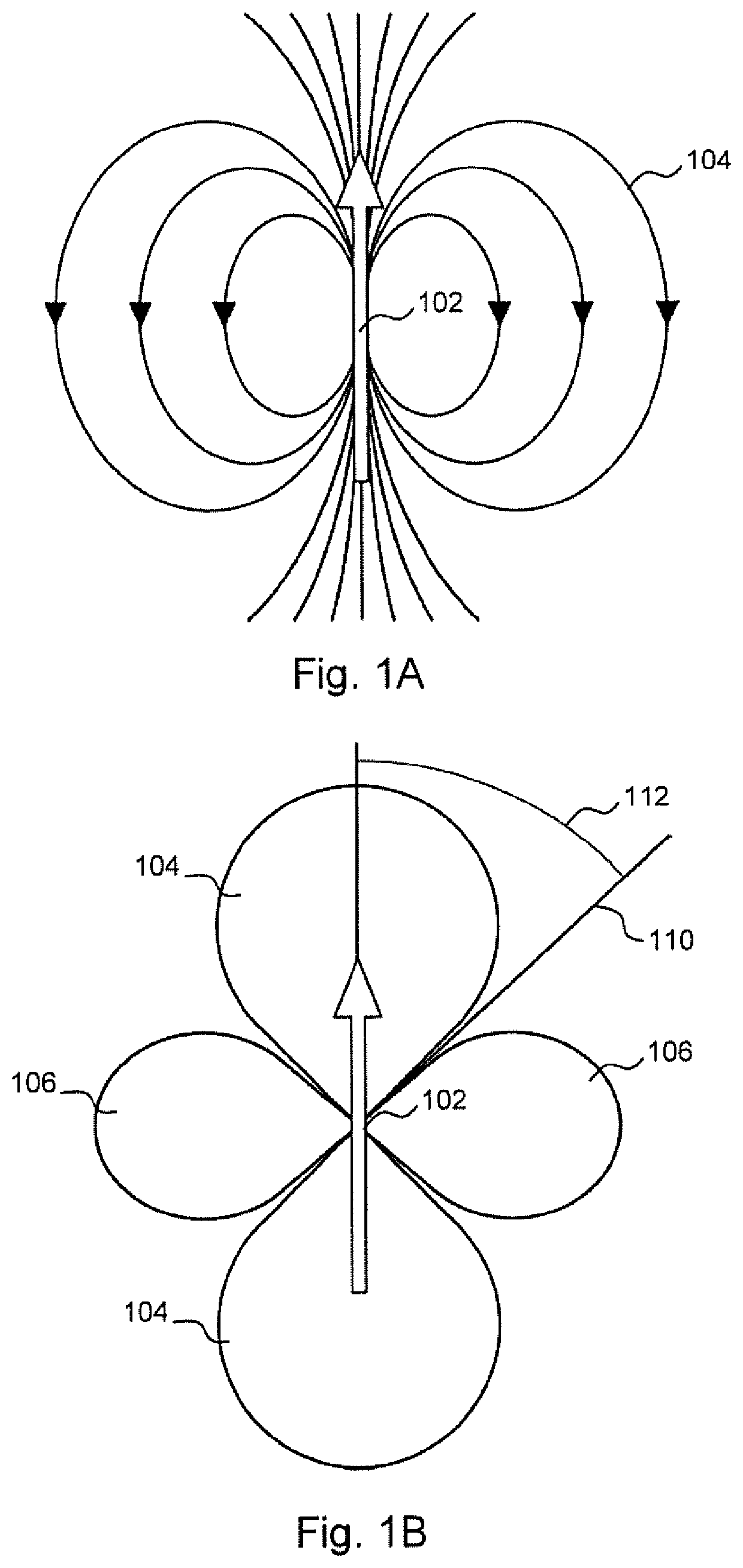
Figure 1 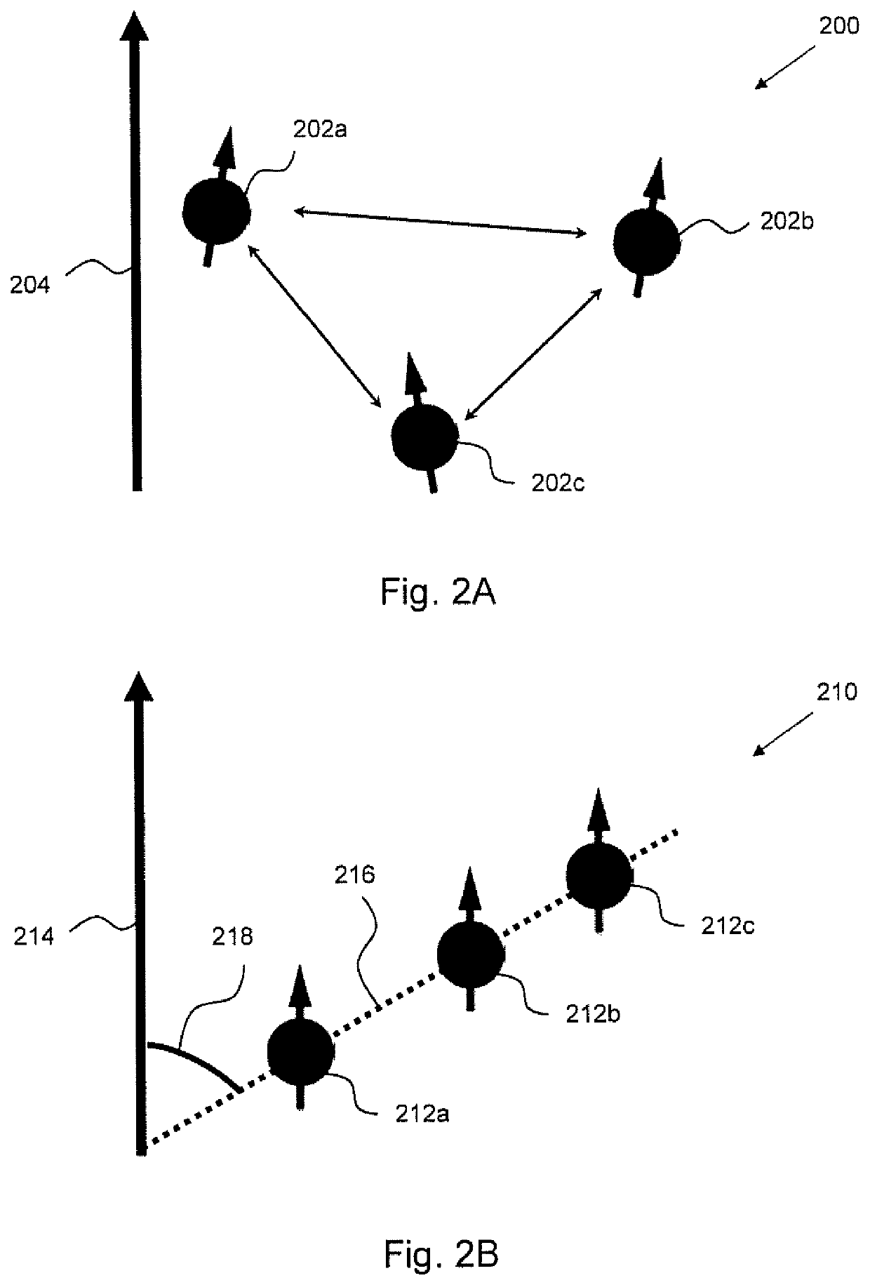
Figure 2 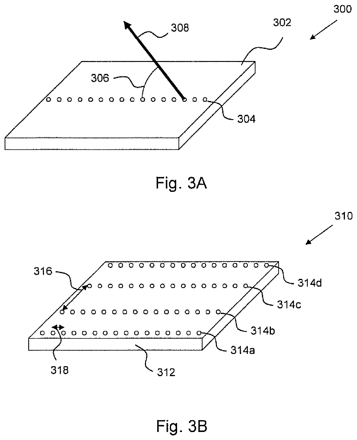
Figure 3
Abstract
Description
TECHNICAL FIELD
[0001] The present disclosure relates to a magnetometer and to a method of detecting a magnetic field.BACKGROUND
[0002] U.S. Pat. No. 8,947,080 (Lukin et al), the contents of which are incorporated herein by reference, describes a magnetometer which includes a solid state electronic spin system and a detector. The solid state electronic spin system contains a plurality of electronic spins that are disposed at locations within a solid carrier which in that case is a single crystal diamond lattice supported by a suitable support structure within the magnetometer, for example attached to an optical waveguide 610 (see FIG. 6 of U.S. Pat. No. 8,947,080). Furthermore, each electronic spin is substantially free of magnetic interference from the carrier, particularly the remainder of the diamond lattice.
[0003] The spins disclosed in U.S. Pat. No. 8,947,080 are nitrogen vacancy (NV) centres within the diamond lattice. An NV centre is a crystallographic defect in the lattice struct...
Examples
Embodiment Construction
[0022]Solid State Electronic Spin Systems
[0023]Any solid state electronic spin system, including surface and body systems, known or to be developed, can be used in the implementation of the present disclosure.
[0024]Examples of suitable spin systems include molecular spin systems, spin systems based on defects or impurities in inorganic solids, and spin systems based on the electron spins of artificial atoms such as quantum dots.
[0025]Molecular Spin Systems
[0026]In molecular spin systems, the spin is typically localised on a metal ion surrounded by ligands, or delocalised with a region of an organic molecule. In both cases, the solvent environment around the molecule plays a critical role in determining the spin coherence time. Longer coherence times are generally provided by solvents which are essentially free of nuclear spins, such as carbon disulphide (CS2). In particular, a molecular magnet having ligands that are nuclear-spin-free and are soluble in CS2 allowed coherence times o...