
Error reduction in semiconductor processes
a technology of semiconductor processes and errors, applied in the field of photolithography, can solve problems such as failure to solve the problem of resolution failure, one or more dies of the wafer being scrapped fast enough to respond. the effect of reducing costs
Patent Information
- Authority / Receiving Office
- US · United States
- Current Assignee / Owner
- Publication Date
- 2005-01-25
- Estimated Expiration
- Not applicable · inactive patent
Smart Images
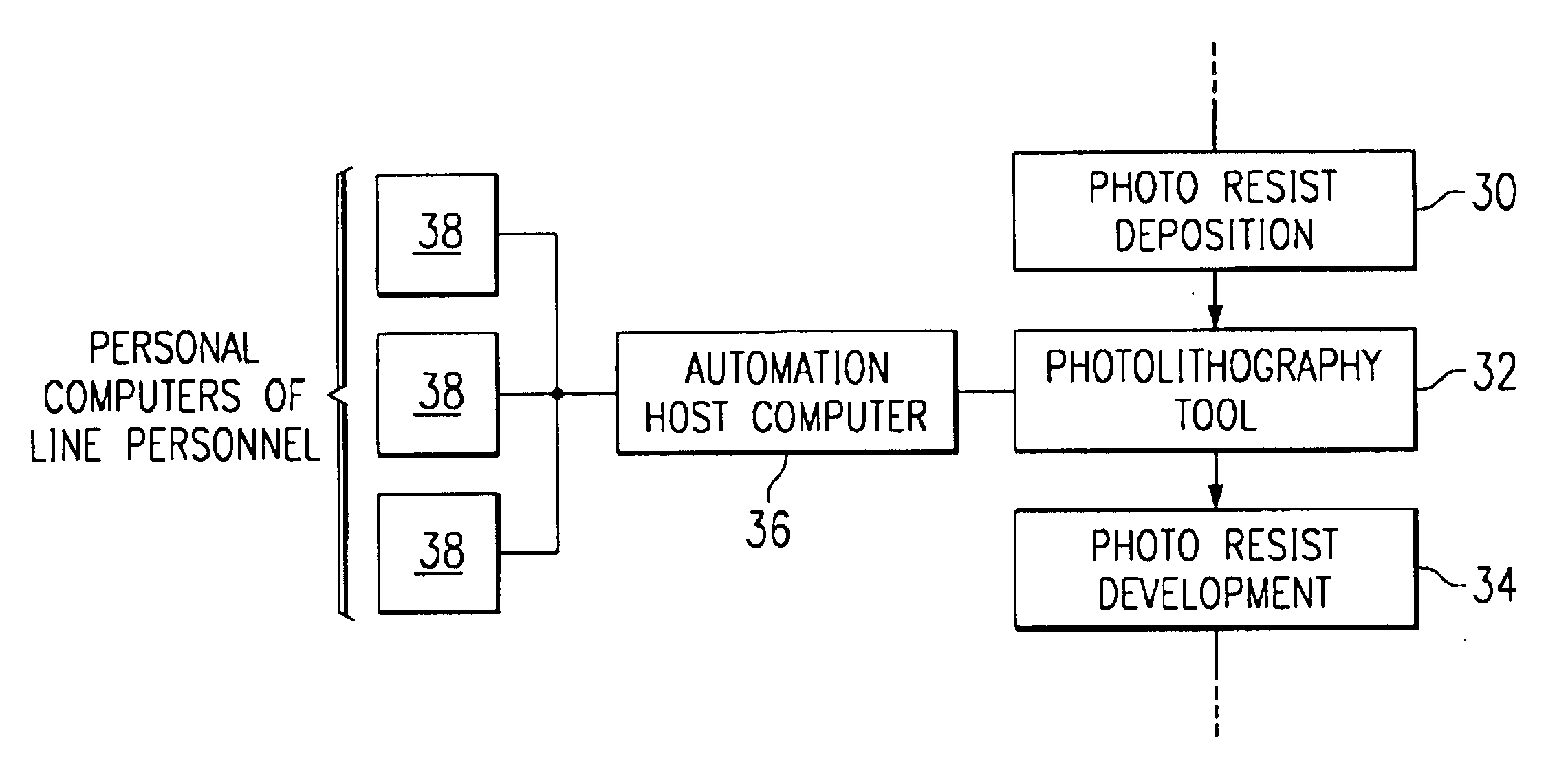
Figure 1 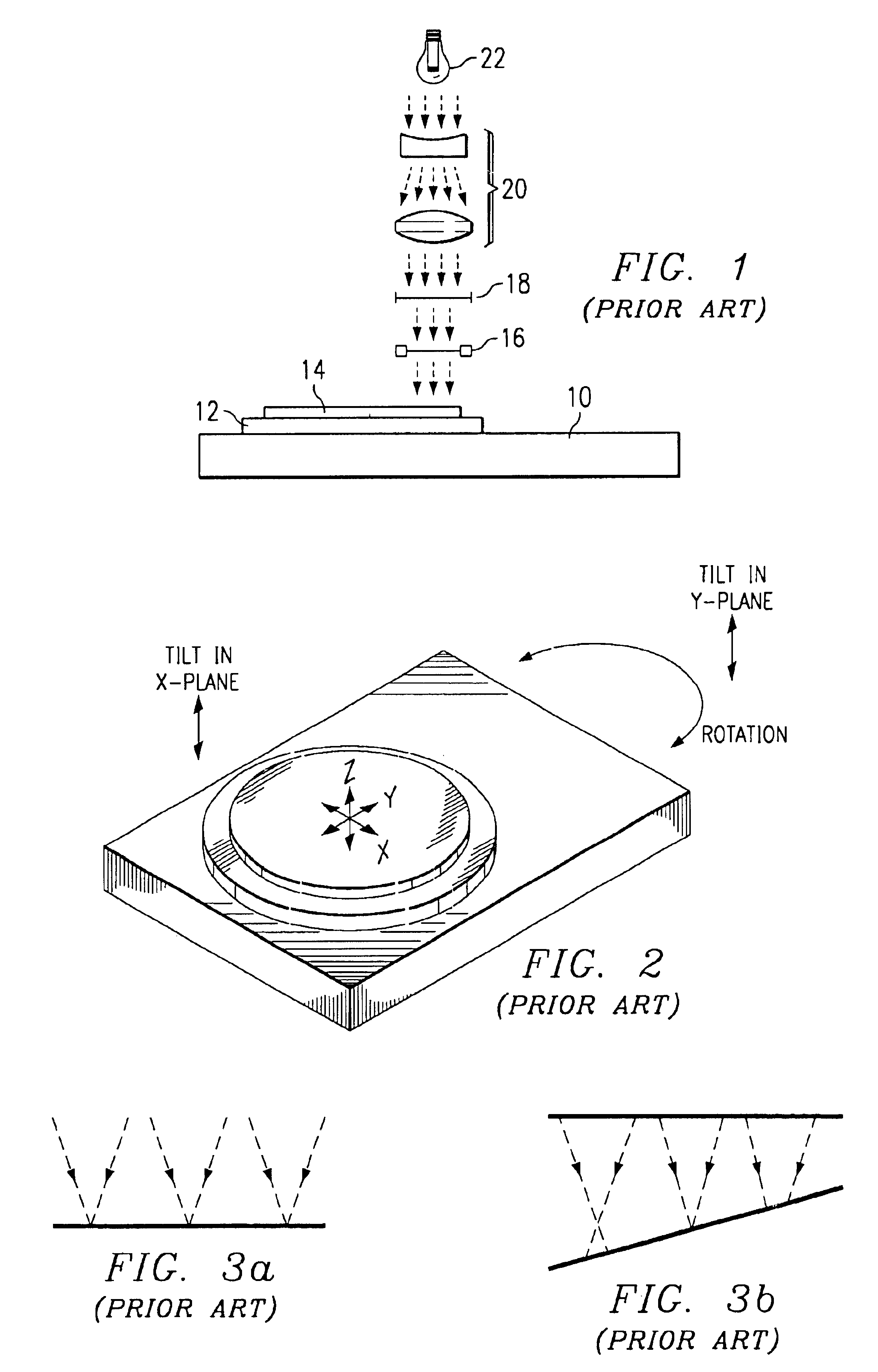
Figure 2 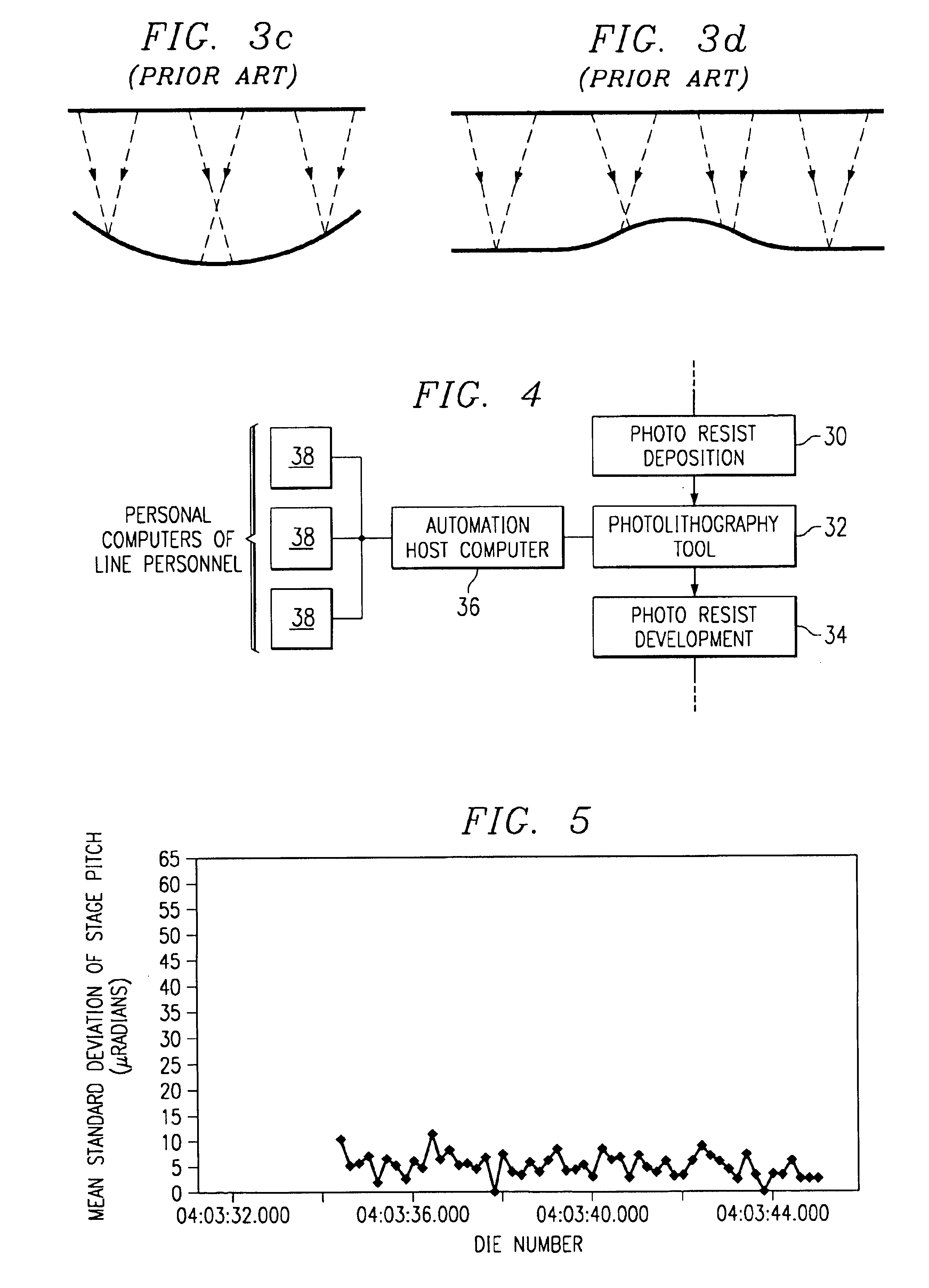
Figure 3
Abstract
Description
BACKGROUND OF THE INVENTIONThis invention is in the field of semiconductor processing, and more particularly in the field of photolithography.In semiconductor processing, photolithography is the process of defining particular features on the surface of a semiconductor wafer. The feature is typically defined with a patterned exposure into a photosensitive material that has been previously deposited on the wafer surface. In a typical photolithographic system, a master pattern image in the form of a photomask or reticle is replicated across the surface of the wafer. The image is typically projected onto the photosensitive material (e.g. photoresist) through a lens system. The quality of the image, and hence the quality and reliability of the resulting feature on the semiconductor surface, is directly related to mechanical parameters such as the spacing and orientation of the lens system relative to the chuck and stage upon which the wafer is placed.Lithography equipment typically inclu...
Examples
Embodiment Construction
FIG. 4 is a block diagram of a portion of a semiconductor integrated circuit fabrication process. The initial block 30 represents the equipment used to deposit, spin, and bake the photoresist onto a wafer. It is followed by the photolithography tool 32 and then by the equipment 34 dedicated to photoresist development. An automation host computer 36 is coupled to the photolithography tool and is also coupled to the personal computers 38 of relevant line management personnel through a local area network, for example.
In one embodiment of the invention, data recording the movement of the stage as the tool 32 seeks to maintain focus as it steps or scans are used to detect die-to-die, wafer-to-wafer, and lot-to-lot defects or errors that have an adverse effect on yield. The automation host computer 36, which controls the tool, reacts to detection of such problems by generating an alert signal and by taking an action specified in an action look-up table, for example. The severity of the pr...