
Semiconductor device having external contact terminals and method for using the same
a technology of contact terminals and semiconductor devices, which is applied in the direction of individual semiconductor device testing, coupling device connection, instruments, etc., can solve the problems of increasing electric contact resistance, inaccurate transmission of test signals, and difficulty in completely removing dirt once adhered
Patent Information
- Authority / Receiving Office
- US · United States
- Patent Type
- Patents(United States)
- Current Assignee / Owner
- Publication Date
- 2006-04-11
- Estimated Expiration
- Not applicable · inactive patent
Smart Images
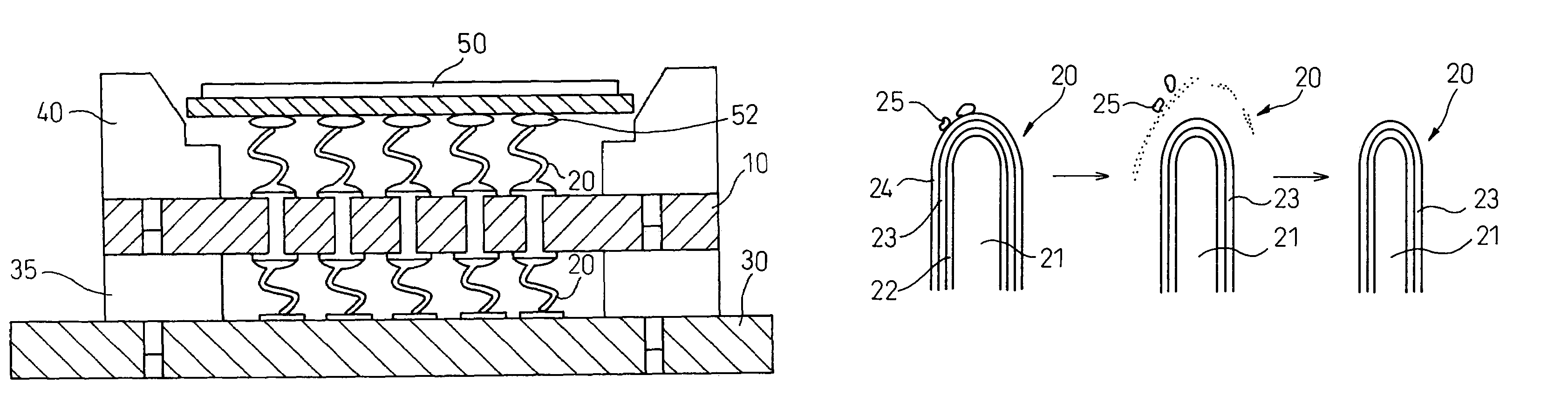
Figure 1 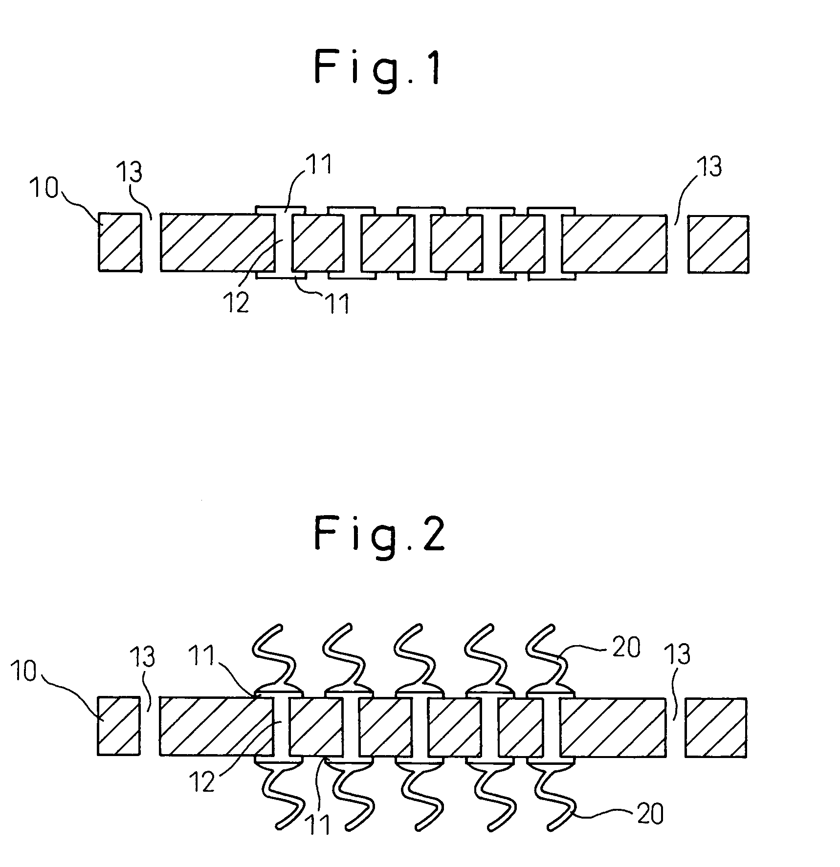
Figure 2 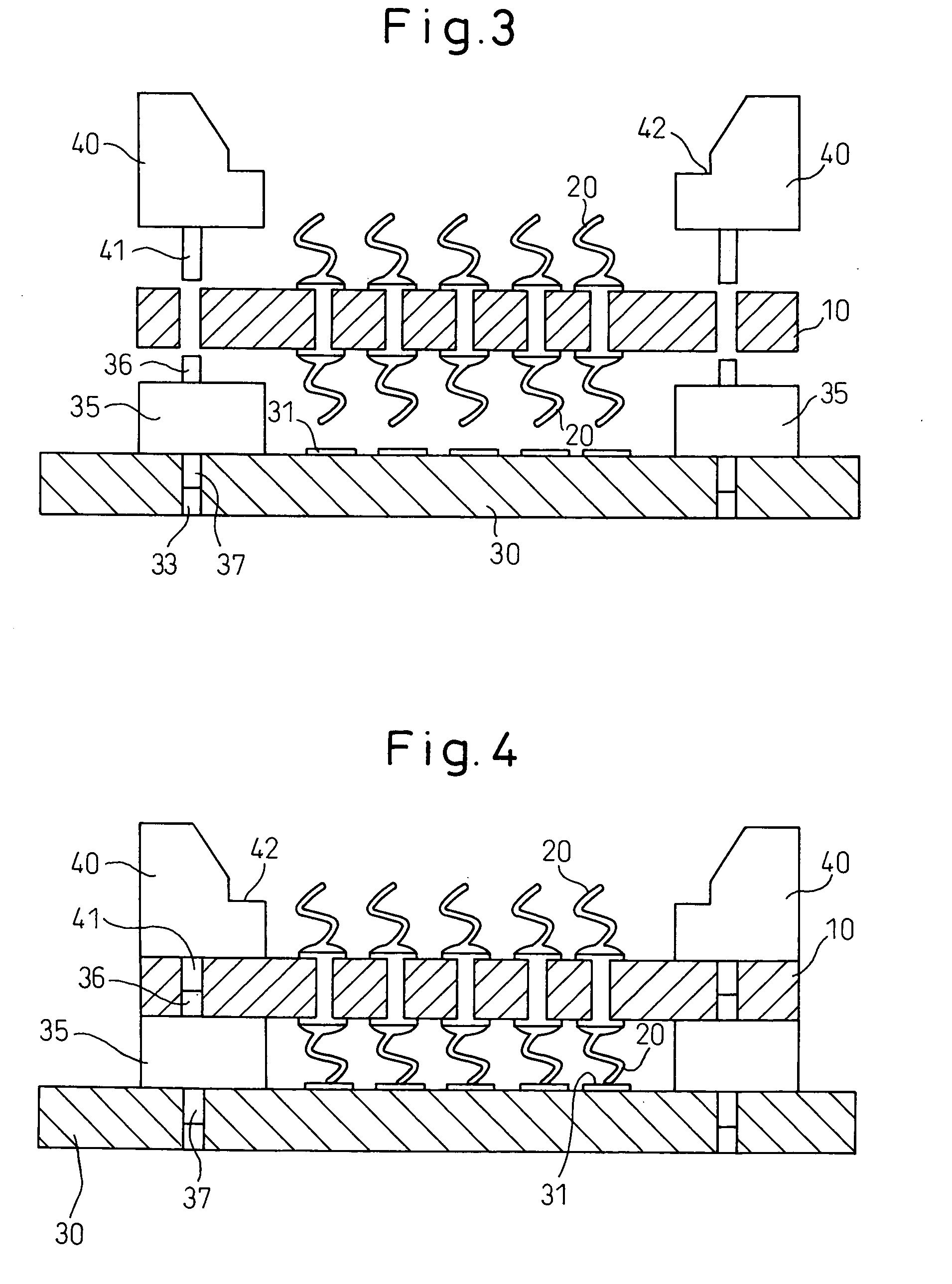
Figure 3
Abstract
Description
BACKGROUND OF THE INVENTION
[0001] 1. Field of the Invention
[0002] The present invention relates to a semiconductor device having external contact terminals and a method for using the same and, particularty to a semiconductor device having external terminals, such as a semiconductor socket having a number of springy external contact pins or terminals of a micro-spring system, which are used while being brought into contact with pads or solder balls of an interposer or a connector board.
[0003] 2. Description of the Related Art
[0004] In the prior art, in a semiconductor device having a number of springy external contact pins or terminals of a micro-spring type, used as a test probe or otherwise, the external contact pin or terminal is made, for example, of a gold (Au) wire for bonding, which surface is plated with palladium (Pd), indium (in) or others. In such a semiconductor device, while the contact terminals repeat making contact with pads or solder balls on an interposer or a connector...
Examples
Embodiment Construction
[0025]Embodiments of the present invention will be described in detail, below, with reference to the attached drawings.
[0026]FIGS. 1 to 4 illustrate a series of processes for producing the inventive semiconductor device having external contact terminals. First, in FIG. 1, a support board 10 is prepared, in which conductor pads 11 and wirings 12 are provided for forming micro-springs (external contact pins of terminals). This support board 10 may be any of various boards generally used as a board for a semiconductor device, such as a glass-epoxy resin board or a ceramic board.
[0027]In general, a number of conductor pads 11 for forming the micro-springs are arranged both on front and back surfaces of the support board in the X direction and the Y direction at a pitch. The wirings 12 are connected to the conductor pads 11, respectively. There are through-hole wirings among the wirings 12, for connecting the conductor pads 11 respectively formed on the front and back surfaces of the sup...