
Semiconductor device
a semiconductor device and mosfet technology, applied in the field of mosfet devices, can solve the problems of difficult to improve the avalanche capability of super junction mosfets with trench gate structures, and achieve the effect of improving the avalanche capability of semiconductor devices
Patent Information
- Authority / Receiving Office
- US · United States
- Patent Type
- Patents(United States)
- Current Assignee / Owner
- Publication Date
- 2010-04-06
Smart Images
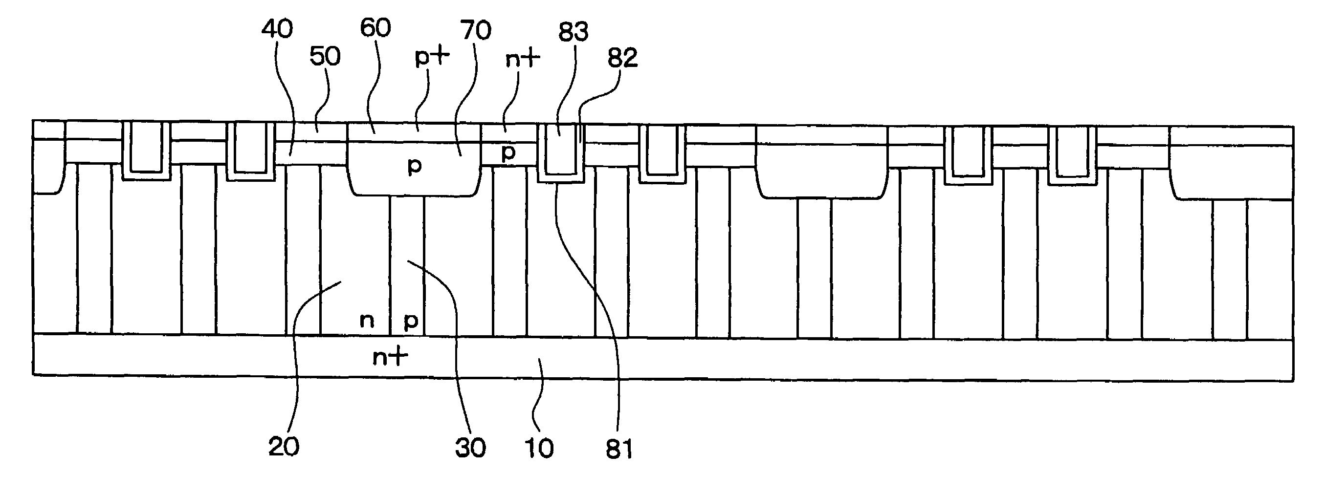
Figure 1 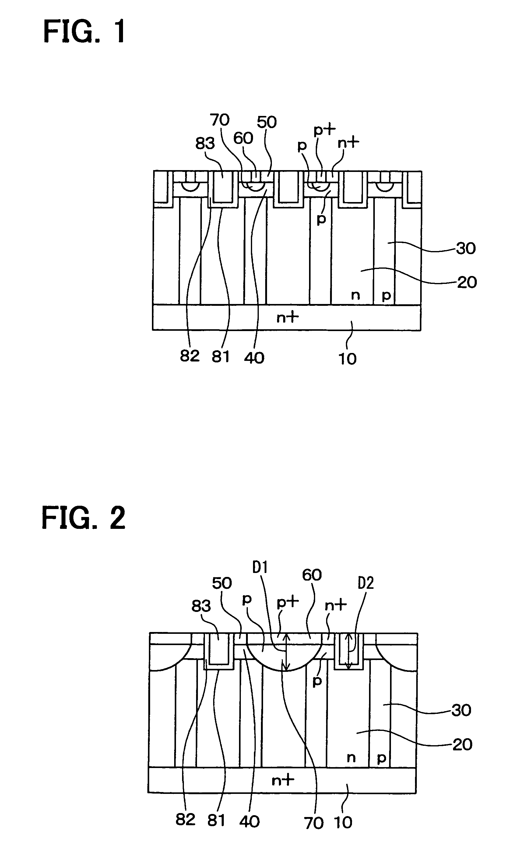
Figure 2 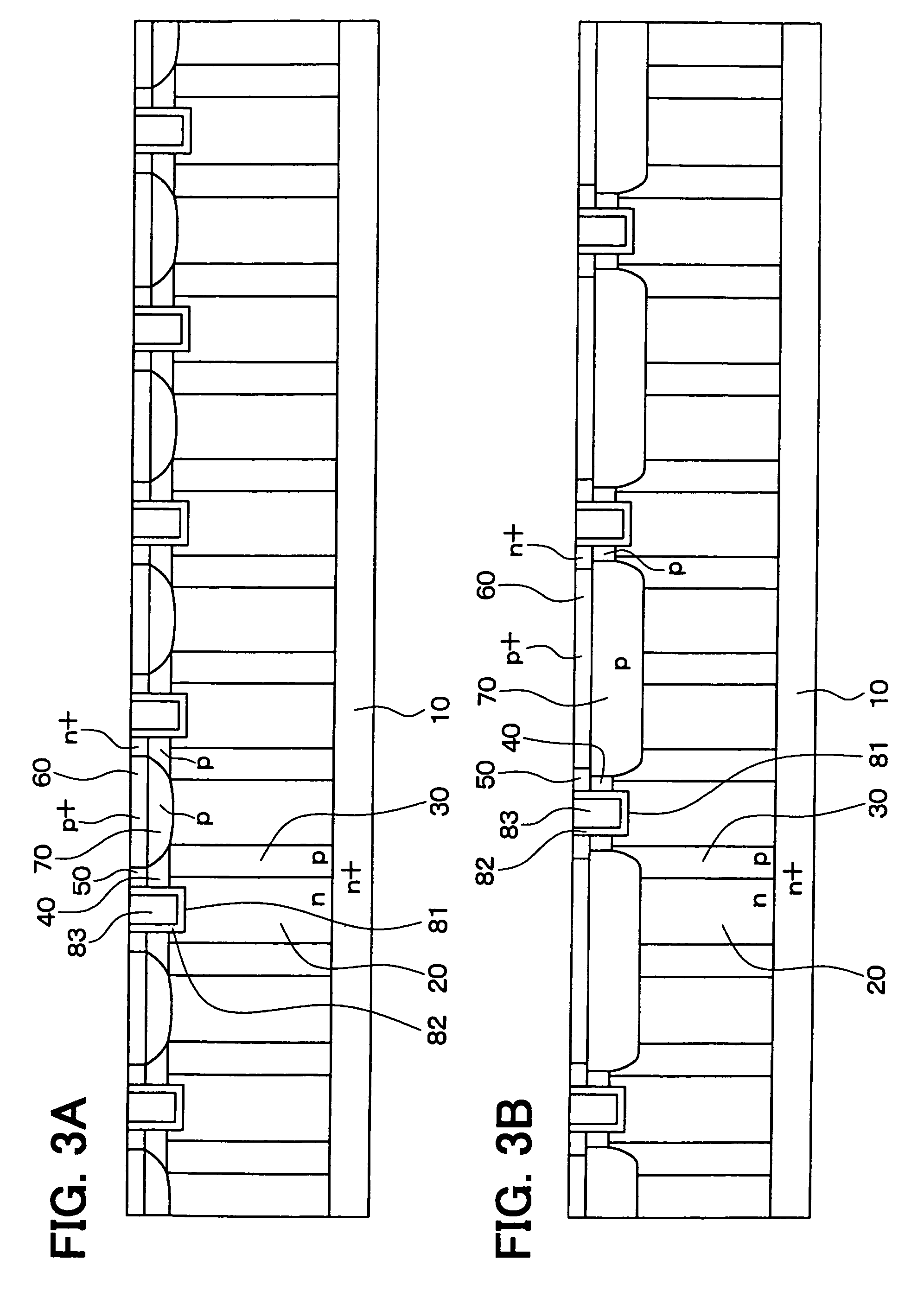
Figure 3
Abstract
Description
CROSS REFERENCE TO RELATED APPLICATION
[0001] This application is based on and incorporates herein by reference Japanese Patent Application No. 2007-131504 filed on May 17, 2007.FIELD OF THE INVENTION
[0002] The present invention relates to a semiconductor device having a trench gate type semiconductor element formed to a semiconductor substrate with a super junction structure.BACKGROUND OF THE INVENTION
[0003] As disclosed in, for example, U.S. Pat. No. 6,734,496 corresponding to JP-A-H9-266311, a super junction metal oxide semiconductor field-effect transistor (MOSFET) has been proposed that achieves improved breakdown voltage and improved on-resistance. In the super junction MOSFET, a drift region is constructed with n-type drift regions and p-type compartment regions that are alternately arranged. Each of the p-type compartment regions is positioned between adjacent n-type drift regions to form a p-n junction. When the MOSFET is in an ON condition, a drift current flows through the n-...
Examples
first embodiment
[0020]A super junction semiconductor device according to a first embodiment of the present invention is described below with reference to the drawings. For example, the semiconductor device can be used as a switching device for an inverter circuit.
[0021]FIG. 1 is a diagram illustrating a cross-sectional view of the semiconductor device according to the first embodiment. As shown in FIG. 1, a column-shaped n-type region 20 and a column-shaped p-type region 30 are formed on a front surface of an n+-type substrate 10. The column-shaped n-type region 20 and the column-shaped p-type region 30 are alternately arranged in a plane direction of the substrate 10 to form a super junction structure (i.e., super junction layer). The column-shaped n-type region 20 and the column-shaped p-type region 30 are hereinafter called “n-column 20” and “p-column 30”, respectively.
[0022]The substrate 10 has an impurity concentration of from about 1×1019 cm−3 to about 1×1020 cm−3. Each of the n-column 20 and...
second embodiment
[0038]A super junction semiconductor device according to a second embodiment of the present invention is described below with reference to FIG. 2. Differences between the first and second embodiments are as follows. In the first embodiment, one trench gate structure is formed to each column structure, which consists of one n-column 20 and one p-column 30 located adjacent to the one n-column 20. In the second embodiment, one trench gate structure is formed to every multiple column structures.
[0039]FIG. 2 is a diagram illustrating a cross-sectional view of the semiconductor device according to the second embodiment. As shown in FIG. 2, an n-column 20 to which a trench gate structure is formed and an n-column 20 to which a trench gate structure is not formed are alternately arranged. In other words, one trench gate structure is formed to every two column structures. Therefore, spacing between adjacent trench gate structures is twice spacing between adjacent column structures. The n-col...
third embodiment
[0045]A super junction semiconductor device according to a third embodiment of the present invention is described below with reference to FIGS. 3A, 3B. Differences between the second and third embodiments are as follows. In the second embodiment, as shown in FIG. 3A, the spacing between adjacent trench gate structures is twice the spacing between adjacent column structures. In the third embodiment, as shown in FIG. 3B, spacing between adjacent trench gate structures is more twice spacing between adjacent column structures.
[0046]For example, as shown in FIG. 3B, in the third embodiment, the spacing between adjacent trench gate structures is three times the spacing between adjacent column structures. In such an approach, two second n-columns 20 can be located between adjacent trench gate structures. Therefore, a p-type body region 70 of the third embodiment can have larger size and depth as compared to that of the second embodiment.
[0047]As the area for the p-type body region 70 is la...