
Silicon carbide MOSFET device with avalanche charge transition buffer layer and preparation method of silicon carbide MOSFET device
A buffer layer and silicon carbide technology, which is applied in semiconductor/solid-state device manufacturing, electrical components, semiconductor devices, etc., can solve problems such as device failure and local temperature rise, so as to slow down local temperature rise, improve avalanche capability, and enhance avalanche reliability effect
Patent Information
- Authority / Receiving Office
- CN · China
- Patent Type
- Applications(China)
- Current Assignee / Owner
- Publication Date
- 2021-08-27
- Estimated Expiration
- Not applicable · inactive patent
Smart Images
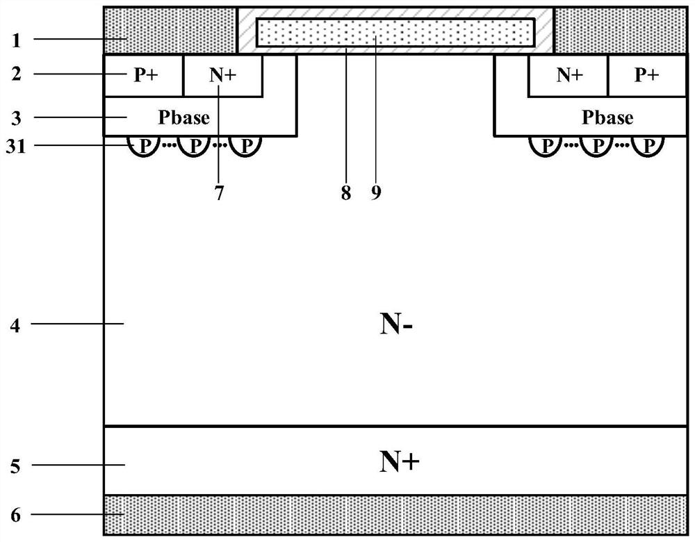
Figure 1 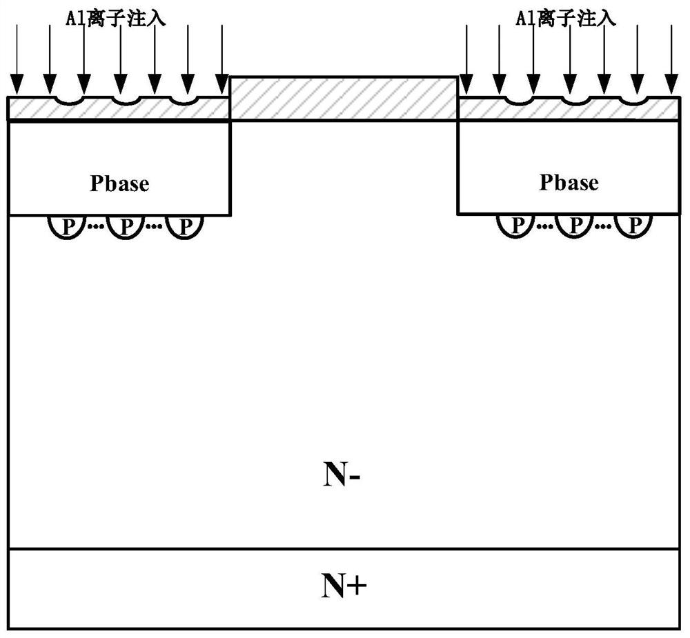
Figure 2 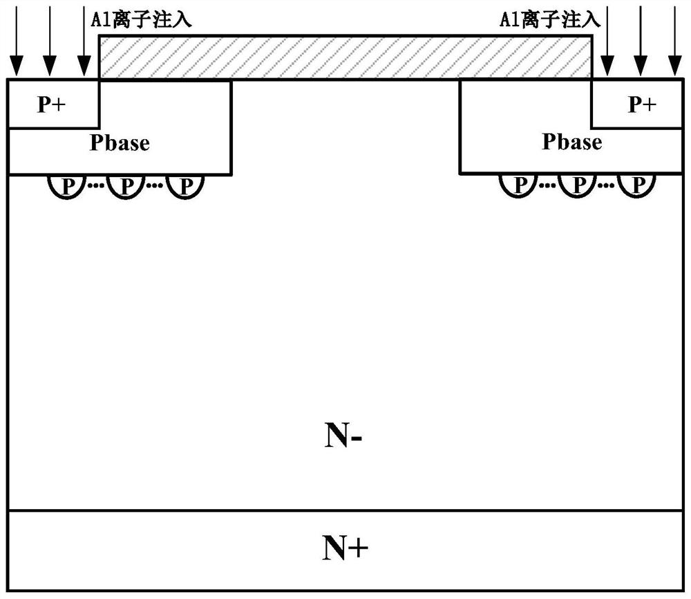
Figure 3
Abstract
Description
technical field
[0001] The invention belongs to the technical field of power semiconductors, in particular to a silicon carbide MOSFET device with an avalanche charge transition buffer layer. Background technique
[0002] Silicon carbide (Silicon Carbide) material, as one of the representatives of the third generation wide bandgap semiconductor materials, has a high breakdown electric field strength (4×10 6 V / cm), high carrier saturation drift velocity (2×10 7 cm / s), high thermal conductivity (490W / m·k), and good thermal stability make it have broad application prospects in the fields of high-power, high-temperature and high-frequency power electronics.
[0003] MOSFET is one of the most widely used devices in silicon carbide power devices. Compared with bipolar devices, silicon carbide MOSFET has lower switching loss and higher frequency characteristics because it has no charge storage effect. As a voltage-type control device, power MOSFET has been widely used in power el...
Examples
Embodiment 1
[0036] like figure 1 As shown, a silicon carbide MOSFET device with an avalanche charge transition buffer layer includes a drain metal 6, an N+ substrate 5 above the drain metal 6, and an N-drift region 4 above the N+ substrate 5; the N - There is a gate dielectric 8 and a polysilicon gate 9 in the middle of the upper part of the drift region 4; a P-type base region 3 is respectively arranged on the upper left and upper right inside the N-drift region 4, and the P-type base region 3 is below the P-type avalanche charge Transition buffer layer 31; the upper left P-type base region 3 includes the upper left P+ ohmic contact region 2, the N+ source region 7 on the right side of the P+ ohmic contact region 2; the upper right P-type base region 3 includes the upper right The P+ ohmic contact region 2, the N+ source region 7 on the left side of the P+ ohmic contact region 2; the source metal 1 above the N+ source region 7 and the P+ ohmic contact region 2; the part of the P-type bas...
Embodiment 2
[0043] like Figure 2-Figure 9 As shown, the present embodiment provides a method for preparing the aforementioned silicon carbide MOSFET device having an avalanche charge transition buffer layer, comprising the following steps:
[0044] The first step: cleaning the epitaxial wafer, N-epitaxial with SiO 2 Implanting aluminum ions into the injection barrier layer to form a P-type avalanche charge transition buffer layer and a P-type base region;
[0045] Step 2: Implant aluminum ions to form P+ ohmic contact area;
[0046]Step 3: Implant nitrogen ions to form N+ source region and activate annealing;
[0047] The fourth step: wet oxygen oxidation to form a gate oxide layer;
[0048] Step 5: Deposit polysilicon, anneal after ion implantation and pattern the polysilicon;
[0049] Step 6: Deposit gate metal to form gate electrode;
[0050] Step 7: thermally grow the isolation oxide layer;
[0051] Step 8: Etching SiO 2 , depositing a source metal to form a source electrode; ...